
User Manual
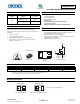


DMN62D0LFB
Document number: DS35409 Rev. 2 - 2
2 of 6
www.diodes.com
October 2011
© Diodes Incorporated
DMN62D0LFB
ADVANCE INFORMATION
NEW PRODUCT
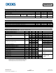
Maximum Ratings @T
A
= 25°C unless otherwise specified
Characteristic Symbol Value Unit
Drain-Source Voltage
V
DSS
60 V
Gate-Source Voltage
V
GSS
±20 V
Continuous Drain Current (Note 4) V
GS
= 4.0V
Steady
State
T
A
= 25°C
T
A
= 70°C
I
D
100
75
mA
Pulsed Drain Current (Note 5)
I
DM
200 mA
Thermal Characteristics
Characteristic Symbol Max Unit
Power Dissipation (Note 4)
P
D
0.47 W
Thermal Resistance, Junction to Ambient @T
A
= 25°C (Note 4) R
JA
258 °C/W
Operating and Storage Temperature Range
T
J
, T
STG
-55 to +150 °C
Electrical Characteristics @ T
A
= 25°C unless otherwise stated
Characteristic Symbol Min Typ Max Unit Test Condition
OFF CHARACTERISTICS (Note 6)
Drain-Source Breakdown Voltage
BV
DSS
60 - - V
V
GS
= 0V, I
D
= 250A
Zero Gate Voltage Drain Current T
J
= 25°C I
DSS
- - 1.0
μA
V
DS
= 60V, V
GS
= 0V
Gate-Source Leakage
I
GSS
- - ±100 nA
V
GS
= ±5V, V
DS
= 0V
- - ±500 nA
V
GS
= ±10V, V
DS
= 0V
- - ±2.0
μA
V
GS
= ±15V, V
DS
= 0V
ON CHARACTERISTICS (Note 6)
Gate Threshold Voltage
V
GS
(
th
)
0.6 - 1.0 V
V
DS
= V
GS
, I
D
= 250A
Static Drain-Source On-Resistance
R
DS (ON)
- 1.3 2
Ω
V
GS
= 4V, I
D
= 100mA
- 1.5 2.5
V
GS
= 2.5V, I
D
= 50mA
- 1.9 3
V
GS
= 1.8V, I
D
= 50mA
- 2.6 -
V
GS
= 1.5V, I
D
= 10mA
Forward Transfer Admittance
|Y
fs
|
- 0.8 - S
V
DS
= 10V, I
D
= 200mA
Diode Forward Voltage
V
SD
- 0.9 1.3 V
V
GS
= 0V, I
S
= 115mA
DYNAMIC CHARACTERISTICS (Note 7)
Input Capacitance
C
iss
- 32 -
pF
V
DS
= 25V, V
GS
= 0V,
f = 1.0MHz
Output Capacitance
C
oss
- 4.4 -
Reverse Transfer Capacitance
C
rss
- 2.9 -
Gate Resistance
R
g
- 126 -
Ω
V
DS
= 0V, V
GS
= 0V, f = 1MHz
Total Gate Charge
Q
g
- 0.45 -
nC
V
GS
= 4.5V, V
DS
= 10V,
I
D
= 250mA
Gate-Source Charge
Q
g
s
- 0.08 -
Gate-Drain Charge
Q
g
d
- 0.08 -
Turn-On Delay Time
t
D
(
on
)
- 3.4 - ns
V
GS
= 10V, V
DS
= 30V,
R
L
= 150, R
G
= 25,
I
D
= 200mA
Turn-On Rise Time
t
r
- 3.4 - ns
Turn-Off Delay Time
t
D
(
off
)
- 26.4 - ns
Turn-Off Fall Time
t
f
- 16.3 - ns
Notes: 4. Device mounted on FR-4 PCB with minimum recommended pad layout, single sided.
5. Repetitive rating, pulse width limited by junction temperature.
6. Short duration pulse test used to minimize self-heating effect.
7. Guaranteed by design. Not subject to production testing.