
User guide


DMP58D0LFB
Document number: DS35206 Rev. 6 - 2
2 of 6
www.diodes.com
September 2012
© Diodes Incorporated
DMP58D0LFB
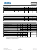
Maximum Ratings (@T
A
= +25°C, unless otherwise specified.)
Characteristic Symbol Value Unit
Drain-Source Voltage
V
DSS
-50 V
Gate-Source Voltage
V
GSS
±20 V
Continuous Drain Current (Note 4) V
GS
= -5V
Steady
State
T
A
= +25°C
T
A
= +70°C
I
D
-180
-150
mA
Continuous Drain Current (Note 5) V
GS
= -5V
Steady
State
T
A
= +25°C
T
A
= +70°C
I
D
-310
-250
mA
Pulsed Drain Current (Note 6)
I
DM
-500 mA
Thermal Characteristics
Characteristic Symbol Max Unit
Power Dissipation (Note 4)
P
D
0.47 W
Thermal Resistance, Junction to Ambient @T
A
= +25°C (Note 4) R
JA
258 °C/W
Power Dissipation (Note 5)
P
D
1.22 W
Thermal Resistance, Junction to Ambient @T
A
= +25°C (Note 5) R
JA
105 °C/W
Operating and Storage Temperature Range
T
J
, T
STG
-55 to +150 °C
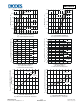
Electrical Characteristics (@T
A
= +25°C, unless otherwise specified.)
Characteristic Symbol Min Typ Max Unit Test Condition
OFF CHARACTERISTICS (Note 7)
Drain-Source Breakdown Voltage
BV
DSS
-50 — — V
V
GS
= 0V, I
D
= -250A
Zero Gate Voltage Drain Current T
J
= 25°C I
DSS
— — -1.0 µA
V
DS
= -50V, V
GS
= 0V
Gate-Source Leakage
I
GSS
— — ±5 µA
V
GS
= ±20V, V
DS
= 0V
ON CHARACTERISTICS (Note 7)
Gate Threshold Voltage
V
GS
(
th
)
-0.8 — -2.1 V
V
DS
= V
GS
, I
D
= -250A
Static Drain-Source On-Resistance
R
DS (ON)
— 6 8
V
GS
= -5V, I
D
= -100mA
— 12 18
V
GS
= -2.5V, I
D
= -10mA
Forward Transfer Admittance
|Y
fs
|
0.05 — — S
V
DS
= -25V, I
D
= -100mA
DYNAMIC CHARACTERISTICS (Note 8)
Input Capacitance
C
iss
— 27 —
pF
V
DS
= -25V, V
GS
= 0V,
f = 1.0MHz
Output Capacitance
C
oss
— 4.0 —
Reverse Transfer Capacitance
C
rss
— 1.4 —
Turn-On Delay Time
t
D
(
on
)
— 30.7 —
ns
V
GS
= -4.5V, V
DS
= -30V,
R
G
= 50, I
D
= -10mA
Turn-On Rise Time
t
r
— 84.1 —
Turn-Off Delay Time
t
D
(
off
)
— 201.8 —
Turn-Off Fall Time
t
f
— 32.2 —
Notes: 4. Device mounted on FR-4 substrate PC board, 2oz copper, with minimum recommended pad layout.
5. Device mounted on FR-4 substrate PC board, 2oz copper, with thermal vias to bottom layer 1inch square copper plate
6. Repetitive rating, pulse width limited by junction temperature.
7. Short duration pulse test used to minimize self-heating effect.
8. Guaranteed by design. Not subject to production testing.