
Owner's manual

LMV331/ LMV393
Document number: DS37022 Rev. 1 - 2
2 of 13
www.diodes.com
May 2014
© Diodes Incorporated
ADVANCED INFORMATION
LMV331/ LM
V
393
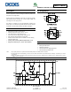
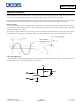
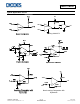
Pin Descriptions
LMV331
Pin Name Pin # Function
IN+ 1 Non-inverting Input
V
EE
2 Chip Supply Voltage(Negative)/GND
IN- 3 Inverting Input
OUT 4 Output
V
CC
5 Chip Supply Voltage(Positive)
LMV393
1OUT 1 Channel 1 Output
1IN- 2 Channel 1 Inverting Input
1IN+ 3 Channel 1 Non-inverting Input
V
EE
4 Chip Supply Voltage(Negative)/GND
2IN+ 5 Channel 2 Non-inverting Input
2IN- 6 Channel 2 Inverting Input
2OUT 7 Channel 2 Output
V
CC
8 Chip Supply Voltage(Positive)
Absolute Maximum Ratings (Note 4) (@T
A
= +25°C, unless otherwise specified.)
Symbol Description Rating Unit
ESD HBM Human Body Model ESD Protection 4.0 KV
ESD MM Machine Model ESD Protection 300 V
Differential Input Voltage ±Supply Voltage V
V
CC
-V
EE
Supply Voltage 5.5 V
θ
JA
Thermal Resistance Junction-to-
Ambient
SOT353 (Note 5) TBD
°C/W
SOT25 (Note 5) TBD
SO-8 (Note 5) TBD
MSOP-8 (Note 5) TBD
T
ST
Storage Temperature -65 to 150 °C
T
J
Maximum Junction Temperature 150 °C
Notes: 4. Stresses greater than the 'Absolute Maximum Ratings' specified above, may cause permanent damage to the device. These are stress ratings only;
functional operation of the device at these or any other conditions exceeding those indicated in this specification is not implied. Device reliability may be
affected by exposure to absolute maximum rating conditions for extended periods of time.
5. All numbers are typical, and apply for packages soldered directly onto a PC board in still air.
Recommended Operating Conditions (@T
A
= +25°C, unless otherwise specified.)
Symbol Description Rating Unit
V
CC
-V
EE
Supply Voltage 2.7 to 5.5 V
T
A
Operating Ambient Temperature Range
-40 to +125
°C