
Manual

MMSTA92
PNP SMALL SIGNAL SURFACE MOUNT TRANSISTOR
Features
• Epitaxial Planar Die Construction
• Complementary NPN Type Available (MMSTA42)
• Ideal for Low Power Amplification and Switching
• Lead Free/RoHS Compliant (Note 2)
• "Green" Device (Notes 3 and 4)
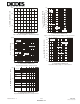
Mechanical Data
• Case: SOT-323
• Case Material: Molded Plastic, "Green" Molding
Compound, Note 4. UL Flammability Classification
Rating 94V-0
• Moisture Sensitivity: Level 1 per J-STD-020C
• Terminal Connections: See Diagram
• Terminals: Solderable per MIL-STD-202, Method 208
• Lead Free Plating (Matte Tin Finish annealed over
Alloy 42 leadframe).
• Marking Information: See Page 3
• Ordering Information: See Page 3
• Weight: 0.006 grams (approximate)
SOT-323
Dim Min Max
A 0.25 0.40
B 1.15 1.35
C 2.00 2.20
D 0.65 Nominal
E 0.30 0.40
G 1.20 1.40
H 1.80 2.20
J 0.0 0.10
K 0.90 1.00
L 0.25 0.40
M 0.10 0.18
α
0° 8°
All Dimensions in mm
E
B
C
A
M
J
L
ED
B
C
H
K
G
BE
C
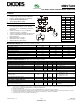
Maximum Ratings @T
A
= 25°C unless otherwise specified
Characteristic Symbol Value Unit
Collector-Base Voltage
V
CBO
-300 V
Collector-Emitter Voltage
V
CEO
-300 V
Emitter-Base Voltage
V
EBO
-5.0 V
Collector Current (Note 1)
I
C
-100 mA
Power Dissipation (Note 1)
P
d
200 mW
Thermal Resistance, Junction to Ambient (Note 1)
R
θ
JA
625
°C/W
Operating and Storage Temperature Range
T
j
, T
STG
-55 to +150
°C
Electrical Characteristics @T
A
= 25°C unless otherwise specified
Characteristic Symbol Min Max Unit Test Condition
OFF CHARACTERISTICS (Note 5)
Collector-Base Breakdown Voltage
V
(BR)CBO
-300
⎯
V
I
C
= -100μA, I
E
= 0
Collector-Emitter Breakdown Voltage
V
(BR)CEO
-300
⎯
V
I
C
= -1.0mA, I
B
= 0
Emitter-Base Breakdown Voltage
V
(BR)EBO
-5.0
⎯
V
I
E
= -100μA, I
C
= 0
Collector Cutoff Current
I
CBO
⎯
-250 nA
V
CB
= -200V, I
E
= 0
Collector Cutoff Current
I
EBO
⎯
-100 nA
V
CE
= -3.0V, I
C
= 0
ON CHARACTERISTICS (Note 5)
DC Current Gain
h
FE
25
40
25
⎯ ⎯
I
C
= -1.0mA, V
CE
= -10V
I
C
= -10mA, V
CE
= -10V
I
C
= -30mA, V
CE
= -10V
Collector-Emitter Saturation Voltage
V
CE(SAT)
⎯
-0.5 V
I
C
= -20mA, I
B
= -2.0mA
Base-Emitter Saturation Voltage
V
BE(SAT)
⎯
-0.9 V
I
C
= -20mA, I
B
= -2.0mA
SMALL SIGNAL CHARACTERISTICS
Output Capacitance
C
cb
⎯
6.0 pF
V
CB
= -20V, f = 1.0MHz, I
E
= 0
Current Gain-Bandwidth Product
f
T
50
⎯
MHz
V
CE
= -20V, I
C
= -10mA,
f = 100MHz
Notes: 1. Device mounted on FR-4 PCB, 1 inch x 0.85 inch x 0.062 inch; pad layout as shown on Diodes Inc. suggested pad layout document AP02001, which
can be found on our website at http://www.diodes.com/datasheets/ap02001.pdf.
2. No purposefully added lead.
3. Diodes Inc.'s "Green" policy can be found on our website at http://www.diodes.com/products/lead_free/index.php.
4. Product manufactured with Date Code 0627 (week 27, 2006) and newer are built with Green Molding Compound. Product manufactured prior to Date
Code 0627 are built with Non-Green Molding Compound and may contain Halogens or Sb2O3 Fire Retardants.
5. Short duration pulse test used to minimize self-heating effect.
DS30174 Rev. 9 - 2 1 of 3
www.diodes.com
MMSTA92
© Diodes Incorporated