
Instruction Manual

TB0640M - TB3500M
Document number: DS30361 Rev. 10 - 2
2 of 6
www.diodes.com
November 2011
© Diodes Incorporated
TB0640M - TB3500M
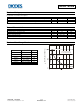
Maximum Ratings @T
A
= 25°C unless otherwise specified
Single phase, half wave, 60Hz, resistive or inductive load.
For capacitance load, derate current by 20%.
Characteristic Symbol Value Unit
Non-Repetitive Peak Impulse Current @10/1000us
I
pp
50 A
Non-Repetitive Peak On-State Current @8.3ms (one-half cycle)
I
TSM
30 A
Typical Positive Temperature Coefficient for Breakdown Voltage
ΔVBR/ΔT
j
0.1 %/°C
Thermal Characteristics
Characteristic Symbol Value Unit
Thermal Resistance, Junction to Lead
R
θ
JL
20 °C/W
Thermal Resistance, Junction to Ambient
R
θ
JA
100 °C/W
Junction Temperature Range
T
J
-40 to +150
°C
Storage Temperature Range
T
STG
-55 to +150
°C
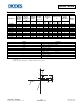
Maximum Rated Surge Waveform
Waveform Standard Ipp (A)
2/10 us GR-1089-CORE 300
8/20 us IEC 61000-4-5 250
10/160 us FCC Part 68 150
10/700 us ITU-T, K.20/K.21 100
10/560 us FCC Part 68 75
10/1000 us GR-1089-CORE 50
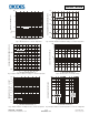
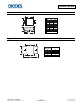
I , PEAK PULSE CURRENT (%)
PP
Peak Value (I )
pp
Half Value
t = rise time to peak value
t = decay time to half value
r
p
t
r
t
p