
Manual

ZLDO485
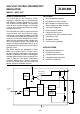
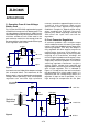
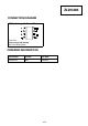
PIN DEFINITIONS
Pin 1 LBF - Low Battery Flag. An open collector
NPN output which pulls low on failing input
supply.
Pin 2 SC - Shutdown Control. This high
impedance logic compatible input disables the
regulator when taken high. It includes a diode
wired to Vin and so will pass current if taken more
than 0.5V above Vin.
Pin 3 Vin - Voltage Input. The power supply to
the regulator. The permissible input voltage
range is -0.3 to 20V. An input capacitor is not
mandatory but will be useful in reducing the
coupling of noise from input to output and
minimising the effect of sudden changes in load
current on the input voltage.
Pin 4 N/C - Not Connected. Not internally
connected and so can be left open or wired to any
pin without affecting the performance of the
regulator.
Pin 5 Vout - Voltage Output. The output of the
regulator. An output capacitor of 1uF or greater
and having low ESR should be wired in close
proximity to the regulator to ensure stability for
all loads.
Pin 6 D/C - Do Not Connect. This pin is wired to
an internal circuit node of the regulator. No
external connection should be made to this pin.
Pin 7 Gnd - Ground. The ground connection of
the regulator against which the output voltage is
referenced.
Pin 8 Spg - Shaping. The shaping node for
the error amplifier of the regulator. A capacitor
of 10pF wired from this pin to the output pin
(pin 5) gives optimum stability. Improved AC
can be achieved by reducing the value of this
capacitor but stability may be impaired for
some load conditions.
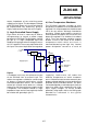
FUNCTIONAL DESCRIPTION
The ZLDO is a high performance, ultra low
dropout, low quiescent regulator. Available in
SM8 surface mount packaging, the device is able
to dissipate 2W(note 1) allowing complete design
flexibility with an input span upto 20V and 300mA
output current. The device quiescent is 1mA (typ)
at 300mA load current. A low battery comparator
signifies impending battery failure, whilst a
shutdown function reduces quiescent current to
a mere 11µA (typ). A precision bandgap
reference gives ± 2.5% output tolerance and
good temperature characteristics over the range
-40 to +85°C. AC performance is enhanced via the
use of a small external capacitor.
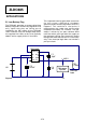
NOTES.
1. Maximum power dissipation of the device is calculated assuming the package is mounted on a PCB
measuring 2 inches square.
2 Output voltage temperature coefficient is calculated as:-
V
O
change
x
1000000
V
O
x
temperature
change
3. Dropout voltage is defined as the input to output voltage differential at which the circuit ceases to
regulate. The value is measured when the output voltage has dropped by 100mV from V
out
measured
at the nominal input V
in
= V
out
+ 1V
4. Guaranteed by design.
4-73