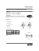
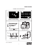
ZXMC3A16DN8 COMPLEMENTARY 30V ENHANCEMENT MODE MOSFET SUMMARY N-Channel V(BR)DSS = 30V; RDS(ON) = 0.035 ; ID= 6.4A P-Channel V(BR)DSS = -30V; RDS(ON) = 0.048 ; ID= -5.4A DESCRIPTION This new generation of trench MOSFETs from Zetex utilizes a unique structure that combines the benefits of low on-resistance with fast switching speed. This makes them ideal for high efficiency, low voltage, power management applications.
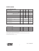
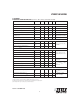
ZXMC3A16DN8 ABSOLUTE MAXIMUM RATINGS PARAMETER SYMBOL Drain-Source Voltage V DSS 30 -30 V Gate-Source Voltage V GS ⫾20 ⫾20 V Continuous Drain Current@V GS =10V; T A =25⬚C (b)(d) @V GS =10V; T A =70⬚C (b)(d) @V GS =10V; T A =25⬚C (a)(d) ID 6.4 5.1 4.9 -5.4 -4.3 -4.1 A A A Pulsed Drain Current (c) I DM 30 -25 A Continuous Source Current (Body Diode) (b) N-Channel P-Channel UNIT IS 3.4 -3.
ZXMC3A16DN8 CHARACTERISTICS ISSUE 1 - OCTOBER 2005 3
ZXMC3A16DN8 N-CHANNEL ELECTRICAL CHARACTERISTICS (at Tamb = 25°C unless otherwise stated) PARAMETER SYMBOL MIN. Drain-Source Breakdown Voltage V (BR)DSS 30 Zero Gate Voltage Drain Current I DSS Gate-Body Leakage I GSS Gate-Source Threshold Voltage V GS(th) TYP. MAX. UNIT CONDITIONS STATIC DYNAMIC I D =250µA, V GS =0V 0.5 µA V DS =30V, V GS =0V 100 nA V GS =±20V, V DS =0V V I =250µA, V DS = V GS D ⍀ ⍀ V GS =10V, I D =9A V GS =4.5V, I D =7.
ZXMC3A16DN8 P-CHANNEL ELECTRICAL CHARACTERISTICS (at Tamb = 25°C unless otherwise stated) PARAMETER SYMBOL MIN. Drain-Source Breakdown Voltage V (BR)DSS -30 Zero Gate Voltage Drain Current I DSS Gate-Body Leakage I GSS Gate-Source Threshold Voltage V GS(th) Static Drain-Source On-State Resistance (1) R DS(on) Forward Transconductance (1)(3) g fs Input Capacitance TYP. MAX. UNIT CONDITIONS STATIC V I D =-250µA, V GS =0V -1.
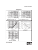
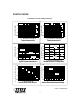
ZXMC3A16DN8 N-CHANNEL TYPICAL CHARACTERISTICS 10V 3V 2.5V 10 1 2V VGS 0.1 1.5V 0.01 0.1 10V T = 150°C 4V ID Drain Current (A) ID Drain Current (A) T = 25°C 1 3.5V 3V 2.5V 4V 10 2V 1 1.5V 0.1 VGS 0.01 1V 10 0.1 VDS Drain-Source Voltage (V) 1 10 VDS Drain-Source Voltage (V) Output Characteristics Output Characteristics 10 Normalised RDS(on) and VGS(th) ID Drain Current (A) 1.6 T = 150°C T = 25°C 1 VDS = 10V 0.1 1 2 3 RDS(on) 1.2 1.0 0.8 VGS(th) 0.
ZXMC3A16DN8 N-CHANNEL TYPICAL CHARACTERISTICS 10 VGS = 0V f = 1MHz 1000 VGS Gate-Source Voltage (V) C Capacitance (pF) 1200 800 600 CISS COSS CRSS 400 200 0 0.1 1 10 VDS - Drain - Source Voltage (V) Capacitance v Drain-Source Voltage ISSUE 1 - OCTOBER 2005 7 ID = 3.
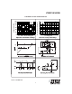
ZXMC3A16DN8 P-CHANNEL TYPICAL CHARACTERISTICS -ID Drain Current (A) 4V T = 150°C 3.5V 3V 2.5V 10 -ID Drain Current (A) 10V T = 25°C 2V 1 -VGS 0.1 1.5V 0.01 0.1 1 3.5V 3V 2.5V 2V 1 1.5V -VGS 0.1 0.01 10 4V 10V 10 0.1 -VDS Drain-Source Voltage (V) 1 10 -VDS Drain-Source Voltage (V) Output Characteristics Output Characteristics 1.6 T = 150°C T = 25°C 1 -VDS = 10V 0.1 1 2 VGS = -10V ID = -4.2A 1.4 Normalised RDS(on) and VGS(th) -ID Drain Current (A) 10 RDS(on) 1.2 1.
ZXMC3A16DN8 P-CHANNEL TYPICAL CHARACTERISTICS 10 VGS = 0V f = 1MHz 1200 -VGS Gate-Source Voltage (V) C Capacitance (pF) 1400 1000 CISS 800 600 COSS CRSS 400 200 0 0.1 1 10 -VDS - Drain - Source Voltage (V) Capacitance v Drain-Source Voltage -ID = 4.
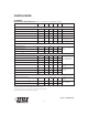
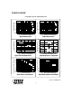
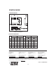
ZXMC3A16DN8 PACKAGE OUTLINE CONTROLLING DIMENSIONS ARE IN INCHES APPROX IN MILLIMETERS PACKAGE DIMENSIONS Millimeters Inches DIM Millimeters Inches DIM Min Max Min Max Min Max A 1.35 1.75 0.053 0.069 e A1 0.10 0.25 0.004 0.010 b 0.33 0.51 0.013 0.020 D 4.80 5.00 0.189 0.197 c 0.19 0.25 0.008 0.010 H 5.80 6.20 0.228 0.244 ⍜ 0° 8° 0° 8° E 3.80 4.00 0.150 0.157 h 0.25 0.50 0.010 0.020 L 0.40 1.27 0.016 0.050 - - - - - 1.27 BSC Min Max 0.