
User guide


ZXMN2A01E6
ISSUE 3 - FEBRUARY 2006
2
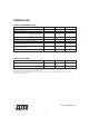
PARAMETER SYMBOL VALUE UNIT
Junction to Ambient (a)
R
θJA
113 °C/W
Junction to Ambient (b)
R
θJA
70 °C/W
NOTES
(a) For a device surface mounted on 25mm x 25mm FR4 PCB with high coverage of single sided 1oz copper, in still air conditions
(b) For a device surface mounted on FR4 PCB measured at t⭐10 secs.
(c) Repetitive rating 25mm x 25mm FR4 PCB, D = 0.05, pulse width 10s - pulse width limited by maximum junction temperature. Refer to
Transient Thermal Impedance graph.
THERMAL RESISTANCE
PARAMETER SYMBOL LIMIT UNIT
Drain-Source Voltage V
DSS
20 V
Gate Source Voltage V
GS
12 V
Continuous Drain Current V
GS
=10V; T
A
=25°C (b)
V
GS
=10V; T
A
=70°C (b)
V
GS
=10V; T
A
=25°C (a)
I
D
3.1
2.5
2.5
A
Pulsed Drain Current (c) I
DM
11 A
Continuous Source Current (Body Diode) (b) I
S
2.4 A
Pulsed Source Current (Body Diode) (c) I
SM
11 A
Power Dissipation at T
A
=25°C (a)
Linear Derating Factor
P
D
1.1
8.8
W
mW/°C
Power Dissipation at T
A
=25°C (b)
Linear Derating Factor
P
D
1.7
13.6
W
mW/°C
Operating and Storage Temperature Range T
j
:T
stg
-55 to +150 °C
ABSOLUTE MAXIMUM RATINGS