
Instruction Manual
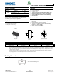

ZXMP6A13FQ
Document Number DS36684 Rev. 2 - 2
2 of 8
www.diodes.com
December 2013
© Diodes Incorporated
ZXMP6A13FQ
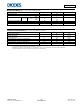
Maximum Ratings (@T
A
= +25°C, unless otherwise specified.)
Characteristic Symbol Value Units
Drain-Source Voltage
V
DSS
-60 V
Gate-Source Voltage
V
GS
±20 V
Continuous Drain Current
V
GS
= 10V
(Note 7)
T
A
= +70°C (Note 7)
(Note 6)
I
D
-1.1
-0.8
-0.9
A
Pulsed Drain Current (Note 8)
I
DM
-4.0 A
Continuous Source Current (Body Diode) (Note 7)
I
S
-1.2 A
Pulsed Source Current (Body Diode) (Note 8)
I
SM
-4.0 A
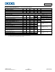
Thermal Characteristics (@T
A
= +25°C, unless otherwise specified.)
Characteristic Symbol Value Unit
Power Dissipation (Note 6)
Linear Derating Factor
P
D
625
5
mW
mW/°C
Power Dissipation (Note 7)
Linear Derating Factor
P
D
806
6.5
mW
mW/°C
Thermal Resistance, Junction to Ambient (Note 6)
R
θJA
200 °C/W
Thermal Resistance, Junction to Ambient (Note 7)
R
θJA
155 °C/W
Thermal Resistance, Junction to Leads (Note 9)
R
θJL
194 °C/W
Operating and Storage Temperature Range
T
J,
T
STG
-55 to +150 °C
Notes: 6. For a device surface mounted on 25mm x 25mm FR4 PCB with high coverage of single sided 1oz copper, in still air conditions
7. For a device surface mounted on FR4 PCB measured at t ≤ 5 secs.
8. Repetitive rating 25mm x 25mm FR4 PCB, D = 0.05 pulse width = 10μs - pulse current limited by maximum junction temperature.
9. Thermal resistance from junction to solder-point (at the end of the collector lead).