
Instruction Manual
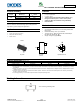

ZXMP6A13FQ
Document Number DS36684 Rev. 2 - 2
4 of 8
www.diodes.com
December 2013
© Diodes Incorporated
ZXMP6A13FQ
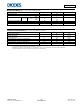
Electrical Characteristics (@T
A
= +25°C, unless otherwise specified.)
Characteristic Symbol Min Typ Max Unit Test Condition
OFF CHARACTERISTICS
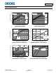
Drain-Source Breakdown Voltage
BV
DSS
-60
V
I
D
= -250μA, V
GS
= 0V
Zero Gate Voltage Drain Current
I
DSS
-0.5 μA
V
DS
= -60V, V
GS
= 0V
Gate-Source Leakage
I
GSS
±100 nA
V
GS
= 20V, V
DS
= 0V
ON CHARACTERISTICS
Gate Threshold Voltage
V
GS
(
th
)
-1.0
-3.0 V
I
D
= -250μA, V
DS
= V
GS
Static Drain-Source On-Resistance (Note 10)
R
DS (ON)
0.4
Ω
V
GS
= -10V, I
D
= -0.9A
0.6
V
GS
= -4.5V, I
D
= -0.8A
Forward Transconductance (Notes 10 and 12)
g
fs
1.8
S
V
DS
= -15V, I
D
= -0.9A
Diode Forward Voltage (Note 10)
V
SD
-0.85 -0.95 V
T
J
= +25°C, I
S
= -0.8A, V
GS
= 0V
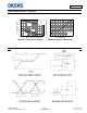
Reverse Recovery Time (Note 12)
t
r
r
21.1
ns
T
J
= +25°C, I
F
= -0.9A,
di/dt = 100A/μs
Reverse Recovery Charge (Note 12)
Q
r
r
19.3
nC
DYNAMIC CHARACTERISTICS (Note 12)
Input Capacitance
C
iss
219
pF
V
DS
= -30V, V
GS
= 0V
f = 1.0MHz
Output Capacitance
C
oss
25.7
Reverse Transfer Capacitance
C
rss
20.5
Turn-On Delay Time (Note 11)
t
D
(
on
)
1.6
ns
V
DD
= -30V, I
D
= -1A,
R
G
6.0Ω V
GS
= -10V
Turn-On Rise Time (Note 11)
t
r
2.2
Turn-Off Delay Time (Note 11)
t
D
(
off
)
11.2
Turn-Off Fall Time (Note 11)
t
f
5.7
Total Gate Charge (Note 11)
Q
g
2.9
nC
V
DS
= -30V, V
GS
= -4.5V,
I
D
= -0.9A
Total Gate Charge (Note 11)
Q
g
5.9
nC
V
DS
= -30V, V
GS
= -10V,
I
D
= -0.9A
Gate-Source Charge (Note 11)
Q
g
s
0.74
Gate-Drain Charge (Note 11)
Q
g
d
1.5
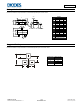
Notes: 10. Measured under pulsed conditions. Pulse width = 300μs. Duty cycle ≤ 2%.
11. Switching characteristics are independent of operating junction temperature.
12. For design aid only, not subject to production testing