
User Manual
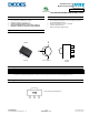

ZXTN4004Z
Document Number: DS35457 Rev: 1 - 2
2 of 5
www.diodes.com
December 2011
© Diodes Incorporated
A
Product Line o
f
Diodes Incorporated
ZXTN4004Z
Maximum Ratings @T
A
= 25°C unless otherwise specified
Characteristic Symbol Value Unit
Collector-Base Voltage
V
CBO
150 V
Collector-Emitter Voltage
V
CEO
150 V
Emitter-Base Voltage
V
EBO
7 V
Continuous Collector Current
I
C
1 A
Peak Pulse Current (Note 4)
I
CM
3 A
Base Current
I
B
500 mA
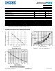
Thermal Characteristics @T
A
= 25°C unless otherwise specified
Characteristic Symbol Value Unit
Power Dissipation (Note 3)
P
D
1.5 W
Thermal Resistance, Junction to Ambient (Note 3)
R
θJA
83
°C/W
Thermal Resistance, Junction to Leads (Note 5)
R
θJL
16.2
°C/W
Operating and Storage Temperature Range
T
J,
T
STG
-55 to +150
°C
Notes: 3. For a device surface mounted on 25mm X 25mm FR4 PCB with high coverage of single sided 1 oz copper, in still air conditions
4. Measured under pulsed conditions. Pulse width = 300µs. Duty cycle ≤ 2%.
5. Thermal resistance from junction to solder-point (on the exposed collector pad).
Thermal Characteristics and Derating Information