
Datasheet


DEM 16217 SYH-LY Product Specification
Version : 5.1.4 PAGE: 4
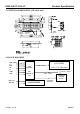
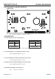
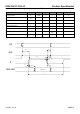
5. PIN ASSIGNMENT
Pin No. Symbol Function
1 VSS Ground terminal of module.
2 VDD Supply terminal of module 2.7V to 5.5V(option 5.0V).
3 V0 Power Supply for liquid crystal drive.
4 RS
Register select
RS = 0…Instruction register
RS = 1…Data register
5 R/W
Read /Write
R/W = 1…Read
R/W = 0…Write
6 E Enable
7 DB0
8 DB1
9 DB2
10 DB3
11 DB4
12 DB5
13 DB6
14 DB7
Bi-directional data bus, data transfer is performed once, thru DB0 to DB7, in the
case of interface data. Length is 8-bits; and twice, thru DB4 to DB7 in the case o
f
interface data length is 4-bits. Upper four bits first then lower four bits.
L- LED – (K) Please also refer to 6.1 PCB drawing and description.
L+ LED + (A) Please also refer to 6.1 PCB drawing and description.