
Specifications

PRODUCT SPECIFICATION
Version 2.4 23 August 2011 16 / 28
The copyright belongs to CHIMEI InnoLux. Any unauthorized use is prohibited.
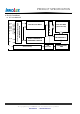
6. INTERFACE TIMING
6.1 TIMING CHARACTERISTICS
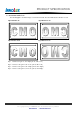
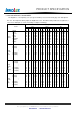
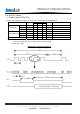
The input signal timing specifications are shown as the following table and timing diagram
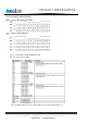
Value
Parameter Symbol
Min. Typ. Max.
Unit
Note
Period Tv 490 500 550 T
h
Tv=Tvd+Tvb
Active Tvd - 480 - T
h
-
Vertical Display
Blanking Tvb 10 20 70 T
h
-
Period T
h
930 992 1090 Tclock
Th=Thd+Thb
Active T
hd
- 800 - Tclock -
Horizontal Display
Blanking T
hb
130 192 290 Tclock -
Clock Frequency 1/T
clock
28 29.5 32 MHz -
Note (1) Since this assembly is operated in DE only mode, Hsync and Vsync input signals should be set to
low logic level. Otherwise, this assembly would operate abnormally.
(2) Frame rate is 60Hz
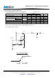
INPUT SIGNAL TIMING DIAGRAM
Data Modul AG - www.data-modul.com