
Specifications

G121SN01 V4 rev. 1.4
P
age 15/24
G
121SN01 V4
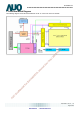
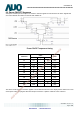
6.3 TFT-LCD Interface Signal Description
The module using a LVDS receiver embaded in AUO’s AS
IC. LVDS is a differential signal technology for LCD
interface and a high-speed data transfer device.
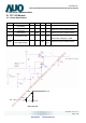
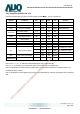
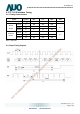
Input Signal Interface
Pin No.
Symbol Description
1 VDD Power Supply, 3.3V (typical)
2 VDD Power Supply, 3.3V (typical)
3 GND Ground
4 SEL68 6/ 8bits LVDS data input selection [H: 8bits L/NC: 6bit]
5 RIN0-
6 RIN0+
LVDS receiver signal channel 0
LVDS Differential Data Input (R0, R1, R2, R3, R4, R5, G0)
7 GND Ground
8 RIN1-
9 RIN1+
LVDS receiver signal channel 1
LVDS Differential Data Input (G1, G2, G3, G4, G5, B0, B1)
10 GND Ground
11 RIN2-
12 RIN2+
LVDS receiver signal channel 2
LVDS Differential Data Input (B2, B3, B4, B5, HS, VS, DE)
13 GND Ground
14 CLKIN-
15 CLKIN+
LVDS receiver signal clock
16 GND Ground
17 RIN3-
18 RIN3+
LVDS receiver signal channel 3, NC for 6 bit LVDS Input
LVDS Differential Data Input (R6, R7, G6, G7, B6, B7, RSV)
19 RSV Reverse Scan Function [H: Enable; L/NC: Disable]
20 NC/GND
Reserved for AUO internal test. Please treat it as NC.
Note 1: Input Signals shall be in low status when VDD is off.
Note 2: High stands for “3.3V”, Low stands for “0V”, NC stands for “No Connection”.
Note 3: RSV stands for “Reserved”.
AUO Confidential For DATAMODUL Internal Use Only / 2012/10/24
Data Modul AG - www.data-modul.com