
User manual


V Panel 104 / 121 / 150 / 170 / 190 User Manual
12
© Copyright Kontron Embedded Computers GmbH
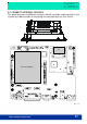
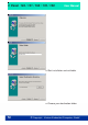
Connector Interface
J3 Serial port COM3
J4 Serial port COM4
J6 Backlight interface
J12 Advanced power button interface
J13 External battery connector
J15 Internal Fieldbus interface
J16 Floppy disk drive interface
J17 Secondary IDE Compact flash
J18 Primary IDE Connector UDMA33
J21 IrDA/FIR connector
J24 PCI extension card
J25 PCMCIA
J26 Internal HDD power interface
J29 4-5 wire Tochconnector
J30 DMC touchcontroller interface (option)
J31/J32 Internal USB interfaces
J34 Speaker interface
J36 ATX Power button
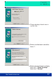
3.3 INTERNAL JUMPER SETTING
To identify the jumper location please look to the board layout in Fig.3.2. All
described functions refers to the implemented baseboard.
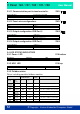
3.3.1 Backlight supply voltage J5
Setting Backlight supply voltage
1-2 (default) 12V
2-3 5V
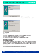
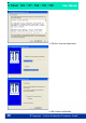
3.3.2 Voltage supplied to display J8
321
456
Setting Display supply voltage
1-6 (default) 3V
2-5 5V
3-4 12V
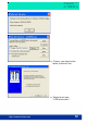
3.3.3 Address range NVSRAM Switch DIP1 SW1
ON
1
OFF
Setting SW1 DIP1 NVSRAM address
OFF CC000 – CFFFF (Hex)
ON D0000 – D7000 (Hex)
*TO ENABLE THE NVSR
A
M DIP8 ON SW1 MUST BE SET TO OFF. IF SJ
A
1000 CHIP SIS POPULATED DIP2 ON SW1 MUST BE SET TO OFF.