DBVT1341 Series A SERVICE MANUAL COLOR TELEVISION/VIDEO CASSETTE RECORDER ORIGINAL MFR’S VERSION B Design and specifications are subject to change without notice.
DBVT1341 SERVICE MANUAL COLOR TELEVISION/VIDEO CASSETTE RECORDER REVISION 1 MFR’S VERSION B MFR’S VERSION IC4001 A LA71200M-MPB B LA71201M-MPB Please file this revision with the original version.
CORRECTION NOTICE MFR'S INCORRECT VERSION REF.NO. A PCB010 CORRECT DESCRIPTION SYSCON PCB ASS'Y VMX210A REF.NO. PCB800 DESCRIPTION SYSCON PCB ASS'Y VMX210A Change of IC ELECTRICAL REPLACEMENT PARTS LIST MFR'S VERSION A PART NO. REF. NO. IC4001 I03F3200M0 IC MFR'S VERSION B DESCRIPTION LA71200M-MPB R1085 PART NO. DESCRIPTION I03F301MN0 IC LA71201M-N-MPB R801R7225J RC 2.2M OHM 1/10W R4018 R903N8822J RC 8.
TAB_SW LDM+ 2.4 2.2 0 7 CAP/M/F/R 8 VCC(5V) C1071 OSD_BLK C1004 100P CH R1036 4.7K 10 CENTLED OSD_B C1023 220P CH C1037 390P CH OSD_G C1067 100P CH 100P CH C1046 20P CH L1001 2.2uH 2.5 R1005 2.7K R1040 C1047 18P CH 33K 42 40 39 38 37 36 35 34 32 31 REC LED TV-POWER T-REC LED 33 RESET-L FROM/TO CHROMA/IF HD X-RAY_TEST VD C-RESET 0 C1040 18P CH 8 AFT_M X1001 12MHz 2.6 2.1 5.2 SDA 1.5 C1050 20P CH 5.2 OSD_BLK RESET AT+5V_BACKUP AT+5V E/V_MASK 4.
SPEC.NO. M578-05A O/R NO.
CHASSIS EXPLODED VIEW (TOP VIEW) 300 502 348 M2003 UN4001 333 334 504 501 335 H5002 342 H5001 336 314 324 341 347 503 315 306 323 331 508 508 305 322 301 302 312 AA 313 AA 332 AA AB AB AA AB M101 318 304 AA 325 309 AA 319 AB 307 AB 506 345 320 AB 346 AB 507 AB 316 317 AB 321 AB AB AB CLASS PART NO. GREASE G-555G MARK AA MG-33 AB I-3 NOTE: Applying positions AA and AB for the grease are displayed for this section.
CHASSIS EXPLODED VIEW (BOTTOM VIEW) 300 303 M2001 AA 510 339 338 AA 510 AA 329 337 AA AA 311 310 AA 509 AA 510 AA 340 AB 308 AB 344 AA 327 343 AA 326 AB 328 AA 505 330 CLASS PART NO. GREASE G-555G MARK AA MG-33 AB I-4 NOTE: Applying positions AA and AB for the grease are displayed for this section. Check if the correct grease is applied for each position.
MECHANICAL REPLACEMENT PARTS LIST REF. NO. PART NO.
CHASSIS REPLACEMENT PARTS LIST REF. NO. 300 PART NO.
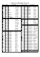
ELECTRICAL REPLACEMENT PARTS LIST REF. NO. ! ! ! ! ! ! ! ! ! ! ! ! ! ! ! ! ! R415 R420 R439 R442 R444 R447 R449 R450 R500 R501 R502 R510 R512 R514 R517 R528 R802 R805 R810 PART NO.
ELECTRICAL REPLACEMENT PARTS LIST REF. NO. PART NO. DESCRIPTION COILS &TRANSFORMERS REF. NO. PART NO.
SPEC.NO. M5A3-03C O/R NO.
A B C D E F G H Y/C/AUDIO/CCD/HEAD AMP SCHEMATIC DIAGRAM (SYSCON PCB) P.CON+5V P.CON+5V 47uH 0305 C D L4005 0.01 F C4060 3.3K 50V 1 KA KA C4067 C4066 0.022 B 50V 1 W818 1.4 17 18 19 20 0 1.5 0.1 2.2 NC 0 16V 10 KA 3.1 2.2K R4062 3.3M C4053 50V 4.7 KA 4.0 C4054 C4057 TU_VIDEO 1 F C4047 FRONT_VIDEO 16V 10 KA C4050 1.6 C4051 2.9 6.3V 33 KA 3.6 R4032 R1025 100 1/4W 100 R4025 C4038 100uH 0305 4 1 Y/C_VIDEO SD_VIDEO 0 DUMMY_V.SYNC 4.9 2.8 2.
A B C D E F MICON SCHEMATIC DIAGRAM FROM TV POWER G H (SYSCON PCB) POWER_FAIL2 C1071 100P CH OSD_BLK CENTLED 1K R1031 R1036 4.
A B C D E F G H IN/OUT SCHEMATIC DIAGRAM (SYSCON PCB) 6 4 GND 3 SOUND_GND FRONT_VIDEO_IN 7 2 SOUND_OUT FRONT_AUDIO_IN 5 1 SP_OUT 173979-7 GND (CD351) CP353_1 FROM/TO OPERATION 9 8 REMOCON_IN 10 8 GND 5 7 4 KEY_A 6 3 T-REC_LED NC AT+5V 2 REC_LED 1 KEY_B 4 (CD757) CP757_2 1-173979-0 3 Y/C VIDEO FROM/TO OPERATION 2 GND 1 1 2 GND AT+5V 3 SCL 173979-4 4 SDA Y/C AUDIO 5 IIC OFF TEST POINT 6 INT-MONI 173979-6 B.
D E F CHROMA/IF SCHEMATIC DIAGRAM W829 11.0 FROM/TO MICON REG. Q603 KTC3203_Y 100 820 1/2W R654 C674 120P CH R668 1K L612 470 1/4W 1M R643 47K 0 17 16 2.8 3.0 UNREG+8V 2.2K VD R648 OSD_BLK C658 R652 0.22 B C688 4.7K C630 0.056 B 100P CH R639 W827 0.1 F C660 4.9 4.9 GND C664 4.8 MKT 2.0 V_OUT HEATER R641 V_FEEDBACK 22K R649 0 180V H_OUT 2.2K H.PLUSE 12K R613 W874 8.0 H_GND 8.0 3.
A B C D E F G H SOUND AMP SCHEMATIC DIAGRAM (SYSCON PCB) 8 8 7 7 FROM/TO IN/OUT W808 SP_OUT SOUND+ SOUND_GND 6 W814 6 8.2 5 3.5 6 0 8 + 4 - 3 5.1 FROM MICON 2 0 5 3.4 7 SOUND AMP IC IC351 AN7511 5 1 0.3 3.9 R359 TV_A_MUTE 47K R353 TV_POWER_H 68K C354 C357 GND 0.001 CH R352 SOUND_GND FROM CHROMA/IF C356 C351 50V 2.2 KA 4.7K SOUND+B 16V 2200 YK FROM TV POWER C355 4 C301 0.0068 B 50V 10 YK 4 R357 AUDIO_OUT 16V 10 KA 3 5.
A B C D E F G H POWER SCHEMATIC DIAGRAM 8 5A 125V (SYSCON PCB) 2.5A 125V 8 CAUTION: FOR CONTINUED PROTECTION AGAINST FIRE HAZARD, REPLACE ONLY WITH THE SAME TYPE FUSE 5A 125V (F501) AND 2.5A 125V (F502) ATTENTION: POUR UNE PROTECTION CONTINUE LES RISQUES D’INCEIE N’UTILISER QUE DES FUSIBLE DE MEME TYPE 5A 125V (F501) ET 2.5A 125V (F502) 7 7 TO SOUND AMP C516 SOUND+B 500V 470P B S802X GND D505 SB290S D515 C521 MTZJ33B F 1 C527 25V 470 YK D507 12 D517 13 14 250V 0.
A B C D E F G H DEFLECTION SCHEMATIC DIAGRAM (SYSCON PCB) 8 8 V.OUTPUT IC IC401 AN5522 THERMAL PROTECTION AMP + PUMP UP GND Vcc 1 7 2 3.6 3 25.9 4 2.0 5 0 6 12.5 7 26.3 7 3.7 V_FEEDBACK C402 R449 5 100V 1 1/2W 0.22 TF C451 MTZJ30B D403 CP401 A1561WV2-A5P 4 W840 3 W857 NC 2 6 1 HS401 763WSAA013 V801 A34JXV70X53N45 W807 GND 5 TO DY MTZJ30B R408 D404 C407 12K C405 R415 17 V_OUT 2.2 FROM/TO CHROMA/IF 1/2W H_CTL 680 1/4W 82K V.POSI VR401 2.
A B C D E F G H CRT SCHEMATIC DIAGRAM (CRT PCB) 8 8 J801_1 HPS3200-010501 0 0 5 0 6 126.5 7 104.1 8 4 3 9 127.5 127.5 1 TP801 BLUE AMP Q804_1 2SC4217 132.5 7 0 F R802 21 7 12K 1W R807 2.8 2.7K 1/4W 2.5 R808 4.7K R814 2.7K 1/4W R811 FROM CHROMA/IF 9 8 7 6 5 NC 4 H_GND 3 HEATER 1 GREEN AMP Q805_1 2SC4217 132.1 470P B 2.9 R805 22 12K 1W 2.5 H_GND1 HEATER 2 5 6 TP802 NC 180V 180V 5 R812 4.
A B C D E F G H OPERATION SCHEMATIC DIAGRAM (OPERATION PCB) 8 8 9 GND 8 AT+5V R777_1 1K 1.5K 1/4W 1 Vout R793_2 EVQ21505R 1/4W REW/REV SW794 5.6K EVQ21505R 1/4W LTL-4224-031A 2 B+ 6 EVQ21505R HEADPHONE_JACK J351 HTJ-035-28A 1 NC 5 7 NC 6 NC 4 R350_1 W815 KEY_A 4 T-REC_LED 6 3 REC_LED 7 2 KEY_B 22 1/4W W805 5 3 5 1 3 GND 270 C755_1 6.3V 220 KA 4.5 R754_2 1/4W R774_1 FF/CUE SW793 EVQ21505R PLAY SW792 2.
A B C D E F G H INTERCONNECTION DIAGRAM 8 8 3 5 2 H H 3 OS753 7 CD352 B+ V.
WAVEFORMS Y/C/AUDIO/CCD/HEAD AMP 1 PB MICON 6 1.0V 20µs/div 0.5V 20µs/div 2 POWER ON POWER ON 7 100mV 0.1µs/div POWER ON 0.5V 10ms/div 11 PB 0.5V 0.5ms/div 13 PB 1.0V 5ms/div DEFLECTION 3 PB 8 PB 9 REC 10.0V 5us/div 18 PB 10.0V 5ms/div 1.0V 10ms/div 0.5V 1ms/div 5 17 0.5V 5ms/div 1.0V 10µs/div 10mV 20us/div 4 POWER ON 10 PB 19 2.0V 20µs/div 1.0V 5ms/div NOTE: The following waveforms were measured at the point of the corresponding balloon number in the schematic diagram.
WAVEFORMS 20 200mV 20µs/div CRT 21 50.0V 20µs/div 22 50.0V 20µs/div 23 50.0V 20µs/div NOTE: The following waveforms were measured at the point of the corresponding balloon number in the schematic diagram.
MECHANICAL EXPLODED VIEW 205 J801 205 111 PCB110 (CRT PCB) 205 L503 205 V801 120 206 116 122 206 206 108 121 207 207 B 117 123 PCB030 (OPERATION PCB) 110 SP351 125 115 118 113 101 I-1
MECHANICAL EXPLODED VIEW 202 114 202 207 202 202 209 203 204 204 106 119 204 202 109 103 208 201 210 105 211 FB401 112 209 211 104 102 104 201 112 PCB010 (SYSCON PCB) 210 204 124 107 I-2
W832 R447 W890 B403 3 W840 C422 W820 C627 C624 C418 C42 B402 01 4 C42 FB401 C432 Q406 W884 HS402 T401 W016 W862 P8 R490 W816 C431 C417 D613 D612 D614 51A CP8 W279 R404 R1064 W054 W056 W823 L1003 C1032 C D402 C402 W817 R453 R460 C433 W828 W863 W280 C1007 W055 C1001 D605 9 00 Q1 CF601 W075 W074 W077 W002 D407 C652 W901 W036 W034 W033 TP601 W037 W872 W007 C659 C612 0 C53 T4001 W082 W897 W080 W087 R505 R532 R533 D501 C4009 W105 R517 D535
F-5 Q404 Q407 Q612 Q611 81 R1009 R4059 C1022 Q1004 C656 C1084 R676 C673 R652 Q608 01 R1045 R1044 C1035 C1031 C1038 C1071 R1048 R1032 R1042 W865 R1087 R1030 51 C1026 31 C1040 C1049 C1048 C1068 C1050 C1046 R1040 C1047 R1005 R1031 C1056 R1033 C1061 R1078 R1034 C1062 C1034 C1083 10 IC R1017 R1029 R1001 R1075 R1038 C1029 R1053 C1025 Q1023 R1021 C1013 R1035 C1009 C1010 C1004 C1023 C1037 R1036 R4047 C4043 R1052 R1019 C1027 Q4007 R1020 Q4009 R1007 Q1024 C1065 R4044 R1025
SERVICING NOTICES ON CHECKING 1. KEEP THE NOTICES 6. AVOID AN X-RAY As for the places which need special attentions, they are indicated with the labels or seals on the cabinet, chassis and parts. Make sure to keep the indications and notices in the operation manual. 2. AVOID AN ELECTRIC SHOCK There is a high voltage part inside. Avoid an electric shock while the electric current is flowing. 3.
CONTENTS SERVICING NOTICES ON CHECKING .................................................................................. HOW TO ORDER PARTS ....................................................................................................... CONTENTS ................................................................................................................................. GENERAL SPECIFICATIONS ....................................................................................................
GENERAL SPECIFICATIONS G-1 TV System CRT CRT Size / Visual Size CRT Type Deflection Magnetic Field BV/BH Video Head 13 inch / 335.4mmV Normal 90 degree +0.45G / 0.18G NTSC 1Speaker Front 1.5 x 2.5 Inch 8 ohm 1.5 W 1.
GENERAL SPECIFICATIONS Timer Rec Set Channel Setup TV/CATV Auto ch Memory Add/Delete Guide ch Set TV Setup V-chip Set On/Off Timer Set Picture Audio Sap On/Off Auto Repeat On/Off On/Off Timer Set System Setup Clock Set Language Auto Clock On/Off Standard Time Daylight Saving Time Commercial Advance Marking On/Off Blueback On/Off Playback Auto/Manual Unmarked Tape Movie Advance Go To Movie Go To Preview G-CODE(or SHOWVIEW or PLUSCODE)No.
GENERAL SPECIFICATIONS 9 0 CH Up CH Down Volume Up Volume Down Input Select Play F.
GENERAL SPECIFICATIONS Important Safeguard Dew/AHC Caution Sheet AC Plug Adapter Quick Set-up Sheet Battery No No No No No UM size x pcs G-15 Interface G-16 G-17 Set Size Weight G-18 Carton G-19 Cabinet Material AC Cord AV Cord (2Pin-1Pin) Registration Card ESP Card 300 ohm to 75 ohm Antenna Adapter Switch Power Play Pause/Still System Select One Touch Playback Channel Up Channel Down F.
DISASSEMBLY INSTRUCTIONS 1-3: TV/VCR BLOCK (Refer to Fig. 1-3) 1. REMOVAL OF MECHANICAL PARTS AND P.C. BOARDS 1. Remove the 2 screws 1. 2. Disconnect the following connectors: (CP757, CP351, CP401 and CP502). 3. Unlock the support 2. 4. Remove the TV/VCR Block in the direction of arrow. 1-1: BACK CABINET (Refer to Fig. 1-1) 1. Remove the 5 screws 1. 2. Remove the AC cord from the AC cord hook 2. 3. Remove the Back Cabinet in the direction of arrow.
DISASSEMBLY INSTRUCTIONS 2. REMOVAL OF DECK PARTS NOTE 2-1: TOP BRACKET (Refer to Fig. 2-1) 1. In case of the Locker R installation, check if the two positions of Fig.2-3-B are correctly locked. 2. When you install the Cassette Side R, be sure to move the Locker R after installing. 1. Extend the 2 supports 1. 2. Slide the 2 supports 2 and remove the Top Bracket. NOTE 1. After the installation of the Top Bracket, bend the support 1 so that the Top Bracket is fixed.
DISASSEMBLY INSTRUCTIONS 2-6: LOADING MOTOR/WORM (Refer to Fig. 2-6-A) 1 1. Remove the screw 1. 2. Remove the Loading Motor. 3. Remove the Worm. Tension Connect Tension Band 1 3 Tension Spring Tension Arm Ass'y Loading Motor Tension Holder 2 4 Worm Main Chassis Fig. 2-7-B • Screw Torque: 3 ± 0.5kgf•cm 1 Fig. 2-6-A NOTE NOTE 1. In case of the Tension Band installation, note the direction of the installation. (Refer to Fig. 2-7-C) 2.
DISASSEMBLY INSTRUCTIONS 2-8: T BRAKE ARM/T BRAKE BAND (Refer to Fig. 2-8-A) 1. Remove the T Brake Spring. 2. Turn the T Brake Arm clockwise and bend the hook section to remove it. 3. Unlock the 2 supports 1 and remove the T Brake Band. Idler Gear Idler Arm Ass'y S Reel T Brake Band (A) 1 Hook section 1 T Reel (A) T Brake Arm 1 T Brake Spring 1 Fig. 2-8-A Fig. 2-9-A NOTE NOTE 1. In case of the S Reel and T Reel installation, check if the correct parts are installed. (Refer to Fig. 2-9-B) 2.
DISASSEMBLY INSTRUCTIONS 2-10: CASSETTE OPENER/PINCH ROLLER BLOCK/ P5 ARM ASS'Y (Refer to Fig. 2-10-A) (1) 1. Unlock the support 1 and remove the Cassette Opener. 2. Remove the Pinch Roller Block and P5 Arm Ass'y. 1 (3) 2 2 2 (2) A/C Head Cassette Opener A/C Head Spring 1 Pinch Roller Block A/C Head Base P5 Arm Ass'y • Screw Torque: 5 ± 0.5kgf•cm (Screw 1) Fig. 2-11-A Spring Position Fig. 2-11-B Main Chassis Fig. 2-10-A NOTE 1. Do not touch the Pinch Roller. (Use gloves.) 2.
DISASSEMBLY INSTRUCTIONS 2-13: AHC ASS'Y/CYLINDER UNIT ASS'Y (Refer to Fig. 2-13) 2-15: MAIN CAM/PINCH ROLLER CAM/JOINT GEAR (Refer to Fig. 2-15-A) 1. Unlock the support 1 and remove the AHC Ass'y. 2. Disconnect the following connector: (CD2001) 3. Remove the 3 screws 2. 4. Remove the Cylinder Unit Ass'y. 1. Remove the E-Ring 1, then remove the Main Cam. 2. Remove the E-Ring 2, then remove the Pinch Roller Cam and Joint Gear. 1 NOTE Main Cam 1.
DISASSEMBLY INSTRUCTIONS 2-18: CASSETTE GUIDE POST/INCLINED BASE S/T UNIT/P4 CAP (Refer to Fig. 2-18-A) NOTE 1. When you install the Loading Arm S Unit, Loading Arm T Unit and Main Loading Gear, align each marker. (Refer to Fig. 2-16-B) 1. Remove the P4 Cap. 2. Unlock the support 1 and remove the Cassette Guide Post. 3. Remove the Inclined Base S Unit and Inclined Base T Unit.
DISASSEMBLY INSTRUCTIONS 3. After one side is removed, pull in the opposite direction to remove the other. 3. REMOVAL OF ANODE CAP Read the following NOTED items before starting work. NOTE * After turning the power off there might still be a potential voltage that is very dangerous. When removing the Anode Cap, make sure to discharge the Anode Cap's potential voltage. * Do not use pliers to loosen or tighten the Anode Cap terminal, this may cause the spring to be damaged.
DISASSEMBLY INSTRUCTIONS 3. When IC starts moving back and forth easily after desoldering completely, pickup the corner of the IC using a tweezers and remove the IC by moving with the IC desoldering machine. (Refer to Fig. 4-3.) 4. REMOVAL AND INSTALLATION OF FLAT PACKAGE IC REMOVAL NOTE 1. Put the Masking Tape (cotton tape) around the Flat Package IC to protect other parts from any damage. (Refer to Fig. 4-1.
DISASSEMBLY INSTRUCTIONS INSTALLATION 4. When bridge-soldering between terminals and/or the soldering amount are not enough, resolder using a Thintip Soldering Iron. (Refer to Fig. 4-8.) 1. Take care of the polarity of new IC and then install the new IC fitting on the printed circuit pattern. Then solder each lead on the diagonal positions of IC temporarily. (Refer to Fig. 4-5.) Thin-tip Soldering Iron IC Soldering Iron Fig. 4-8 5.
KEY TO ABBREVIATIONS A A/C ACC AE AFC AFT AFT DET AGC AMP ANT A.PB APC ASS'Y AT AUTO A/V B BGP BOT BPF BRAKE SOL BUFF B/W C C CASE CAP CARR CH CLK CLOCK (SY-SE) COMB CONV CPM CTL CYL CYL-M CYL SENS D DATA (SY-CE) dB DC DD Unit DEMOD DET DEV E E EF EMPH ENC ENV EOT EQ EXT F F FBC FE FF FG FL SW FM FSC FWD G GEN GND H H.P.
KEY TO ABBREVIATIONS S SYNC SYNC SEP T TR TRAC TRICK PB TP U UNREG V V VCO VIF VP V.PB VR V.
SERVICE MODE LIST This unit provided with the following SERVICE MODES so you can repair, examine and adjust easily. To enter SERVICE MODE, unplug AC cord till lost actual clock time. Then press and hold Vol (-) button of main unit and remocon key simultaneously. The both pressing of set key and remote control key will not be possible if clock has been set. To reset clock, either unplug AC cord and allow at least 5 seconds before Power On. Set Key Remocon Key VOL. (-) MIN 0 Releasing of V-CHIP PASSWORD.
PREVENTIVE CHECKS AND SERVICE INTERVALS The following standard table depends on environmental conditions and usage. Unless maintenance is properly carried out, the following service intervals may be quite shortened as harmful effects may be had on other parts. Also, long term storage or misuse may cause transformation and aging of rubber parts. Time Parts Name 500 hours 1,000 hours 1,500 hours 2,000 hours 3,000 hours Notes Audio Control Head Clean those parts in contact with the tape.
PREVENTIVE CHECKS AND SERVICE INTERVALS CLEANING 2. TAPE RUNNING SYSTEM NOTE When cleaning the tape transport system, use the gauze moistened with isopropyl alcohol. After cleaning the heads with isopropyl alcohol, do not run a tape until the heads dry completely. If the heads are not completely dry and alcohol gets on the tape, damage may occur. 3. CYLINDER Wrap a piece of chamois around your finger. Dip it in isopropyl alcohol. Hold it to the cylinder head softly.
WHEN REPLACING EEPROM (MEMORY) IC If a service repair is undertaken where it has been required to change the MEMORY IC, the following steps should be taken to ensure correct data settings while making reference to TABLE 1. NOTE: Initial Data setting will not be possible if clock has been set. To reset clock, either unplug AC cord and allow at least 5 seconds before Power On.
SERVICING FIXTURES AND TOOLS (For 2 heads model) VHS Alignment Tape JG001 (VN 2 S-LI6 3 ) JG001A (VN 2 S-CO13 ) JG001Q (VN 2 S-LI6 3 H) JG001T (VN 2 S-X6 3 ) (For 4 heads model) VHS Alignment Tape JG001B (VN 1 S-LI6 3 ) JG001I (VN 1 S-CO13 ) JG001P (VN 1 S-LI6 3 H) JG001S (VN 1 S-X6 3 ) JG002B Adapter JG002E Dial Torque Gauge (10~90gf•cm) JG002F (60~600gf•cm) JG005 Post Adjustment Screwdriver Part No.
MECHANICAL ADJUSTMENTS 1-2: CONFIRMATION AND ADJUSTMENT OF TENSION POST POSITION 1. CONFIRMATION AND ADJUSTMENT Read the following NOTES before starting work. 1. Set to the PLAY mode. 2. Adjust the adjusting parts for the Tension Arm position so that the Tension Arm top is within the standard line of Main Chassis. 3. While turning the S Reel clockwise, confirm that the edge of the Tension Arm is located in the position described above.
MECHANICAL ADJUSTMENTS 1-4: CONFIRMATION OF VSR TORQUE NOTE 1. Install the Torque Gauge (JG002F) and Adapter (JG002B) on the S Reel. Set to the Picture Search (Rewind) mode. (Refer to Fig.1-4-B) 2. Then, confirm that it indicates 120~180gf•cm. If the torque is out of the range, replace the following parts. NOTE Check item Replacement Part 1-4 Idler Ass'y/Clutch Ass'y 1-5 Install the Torque Gauge on the reel disk firmly. Press the REW button to turn the reel disk.
MECHANICAL ADJUSTMENTS 2-2: CONFIRMATION AND ADJUSTMENT OF AUDIO/ CONTROL HEAD 2-3: TAPE RUNNING ADJUSTMENT (X VALUE ADJUSTMENT) When the Tape Running Mechanism does not work well, adjust the following items. 1. Confirm and adjust the height of the Reel Disk. (Refer to item 1-1) 2. Confirm and adjust the position of the Tension Post. (Refer to item 1-2) 3. Adjust the Guide Roller. (Refer to item 2-1) 4. Confirm and adjust the Audio/Control Head. (Refer to item 2-2) 5.
MECHANICAL ADJUSTMENTS 3. MECHANISM ADJUSTMENT PARTS LOCATION GUIDE 4 5 6 3 2 7 1 10 9 1. Tension Connect 2. Tension Arm 3. Guide Roller 4. Audio/Control Head 5. X value adjustment driver hole 8 6. 7. 8. 9. 10.
ELECTRICAL ADJUSTMENTS 1. BEFORE MAKING ELECTRICAL ADJUSTMENTS 2. BASIC ADJUSTMENTS (VCR SECTION) Read and perform these adjustments when repairing the circuits or replacing electrical parts or PCB assemblies. 2-1: PG SHIFTER 1. Connect CH-1 on the oscilloscope to TP1002 and CH-2 to pin 4 of CP1003. 2. Playback the alignment tape. (JG001A) 3. Press and hold the Tracking-Auto button on the remote control more than 2 seconds to set tracking to center. 4. Press the VOL.
ELECTRICAL ADJUSTMENTS 2-3: RF AGC 2-8: HORIZONTAL PHASE 1. Receive the VHF HIGH (63dB). 2. Connect the digital voltmeter between the pin 5 of CP351 and the pin 1 (GND) of CP351. 3. Activate the adjustment mode display of Fig. 1-1 and press the channel button (02) on the remote control to select "RF AGC". 4. Press the VOL. UP/DOWN button on the remote control until the digital voltmeter is 2.9V ± 0.05V. (TV SECTION) 1. Receive the center cross signal from the Pattern Generator. 2.
ELECTRICAL ADJUSTMENTS 2-12: SUB CONTRAST MANUAL White 0% 1. Receive the color bar pattern. (RF Input) 2. Using the remote control, set the brightness and contrast to normal position. 3. Activate the adjustment mode display of Fig. 1-1 and press the channel button (14) on the remote control to select "CONTRAST". 4. Press the VOL. UP/DOWN button on the remote control until the contrast STEP No. becomes "100". 5. Receive the color bar pattern. (Audio Video Input) 6.
ELECTRICAL ADJUSTMENTS 3.
ELECTRICAL ADJUSTMENTS 4-3: STATIC CONVERGENCE 4. PURITY AND CONVERGENCE ADJUSTMENTS NOTE Adjust after performing adjustments in section 4-2. NOTE 1. Receive the crosshatch pattern from the color bar generator. 2. Combine red and blue of the 3 color crosshatch pattern on the center of the screen by adjusting the pair of 4 pole magnets. 3. Combine red/blue (magenta) and green by adjusting the pair of 6 pole magnets. 1.
TV BLOCK DIAGRAM V. OUTPUT IC IC401 AN5522 MICON/ OPERATION/ IN/OUT SCL SDA Q602, Q603 AT+5V_BACK UP AT+12V Q604, Q605 Q601 60 11 AFT OUT 33 39 46 13 53 POWER ON CONT FM DIRECT OUT 5V REG MCU RESET 1 2 Q407 H-CONTROL SW PUMP UP 3 5 H_CTL 7 MICON/ OPERATION/ IN/OUT Q406 Q405 SW REG CONT VIF IN 5 NC 42 8.7V REG OUT 64 41 5.
Y/C/AUDIO/CCD/HEAD AMP BLOCK DIAGRAM X4001 3.579545MHz Q4010 Q4012 50 41 49 P NC 66 REC APC L H R R CP4001 1 65 P 2 SP-CH2 (L) 72 P 73 P CLAMP AUTO-BIAS CCD H L R 74 REC APC Main CONV 3 SP_COM 4 SP-CH1 (R) 37 3.58M BPF2 62 HA GND CYL 38 VSS 43 4FSC PLL VX01 NC 67 BUFFER BUFFER Y/C/AUDIO/CCD/HEAD AMP IC IC4001 LA71201M-N-MPB B-UP AMP C-LPF SERAIL DECODER AGC P 53 Y/C_CLK 54 Y/C_DATA 55 Y/C_CS MICON/ OPERATION/ IN/OUT OUT VCA 36 ACC DET VD TV 9 3.
MICON/OPERATION/IN/OUT BLOCK DIAGRAM TIMER SYSCON MICON IC IC1001 OEC7071A SW1001 50 TAB SW 1 3 1 4 1 2 CAPSTAN DD UNIT 1 4 2 2 TV 3 2 MSSEN-B MS_SEN B Q1003 3 4 MSSEN-A MS_SEN A Q1009 80 REEL-T REEL SENS. Q1005 H_CONTROL 24 H_CONTROL X-RAY_TEST 41 X-RAY_TEST VCR_POWER_H 27 VCR-POWER CP1004 12 CAP-LIMIT 76 CAP-PWM 87 CAP-FG 1 4 5 9 10 11 12 34 POWER_FAIL_L 85 X-OUT(12MHz) 39 1 OUT SYSTEM RESET IC IC1003 R3111N311A/C-TR POWER FAIL2 AT+5.6V P.
PRINTED CIRCUIT BOARDS OPERATION SOLDER SIDE R777_1 R775_1 C382 R776_1 W009 W805 SW794 SW792 SW793 SW791 R773_1 R774_1 R771_1 R772_1 W811 R793_2 R778_1 CD352 F-1 CD351_1 R766 OS753 R754_2 CD757 W002 SW796 W001 SW798 W815 W008 W814 R350_1 SW795 J701_1 W003 SW799 W004 W005 SW797 W007 W006 SW751 W812 R351 J351 C755_1 D793 D791 F-2