Price: $30.
Page 2 DZ COMPANY CONTACT INFO Orders, parts, phone assistance.....................................................................(970) 667-7382 Email orders............................................................................................... sales@dzkit.com Email technical support ......................................................................... support@dzkit.com Web site ....................................................................................................... www.dzkit.
Page 3 Service Manual for the TABLE OF CONTENTS Sienna HF Transceiver Troubleshooting ............................... 4 Voltage, Resistance Charts ............... 6 Specifications ................................. 10 Theory of Operation ........................11 Block Diagram ............................... 33 Schematics ..................................... 34 DZ COMPANY LOVELAND, COLORADO Copyright © 2011 The DZ Company.
Page 4 TROUBLESHOOTING The nice thing about building your own transceiver is being able to fix it if it breaks, or to figure out why it’s not working quite right as you turn it on for the first time, WITHOUT having to send it back to us for repair. But we have found that many people lack basic trou‐ bleshooting skills. So here are a few tips to help you narrow down a problem: 1. Start by measuring the main DC voltages on every board.
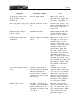
Page 5 Symptom 5v Supply reads low, front panel seems locked up Possible Causes C24 on DCD board Fix Make sure C24 is mounted the right di‐ rection, resolder it. DCD Tray gets very hot Normal without cover on Attach top cover.
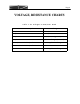
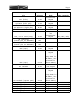
Page 6 VOLTAGE, RESISTANCE CHARTS Table 1. DC Voltages on DCD/Tuner Board Measurement point Voltage J10 pin 1 5.0V +/‐.15V J10 pin 2 ‐9.5V +/‐.5V J10 pins 3 and 5 0.0V +/‐.05V (ground) J10 pin 4 Applied voltage (11‐15V) Anode (unbanded side) of D7 0.25 * applied voltage Cathode (banded side) of D9 and D5 2.7V Junction of R24 and R25 0.
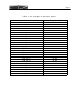
Page 7 Table 2. DC Voltages on Receiver Board Pin J5 pin 1 J5 pin 2 J5 pin 4 J13 pin 4 TP3 U14 pin 1 U13 pin 3 U18 pin 14 U19 pin 14 U4 pin 8 U4 pin 4 U22 pin 8 Q5 gate 1 Q5 source Q5 drain Q20 gate 1 Q20 source Q20 drain U25 pin 7 U30 pin 8 U30 pin 4 U5 pin 8 U9 pin 2 U26 pin 7 U7 pin 8 U11 pin 4 U11 pin 11 Voltage (+/‐5%) +5.0V ‐9.5V +11 to +15V 9.0V >4.0V ‐5.0V +5.0V +11 to +15V +11 to +15V +4.5V ‐9.0V +5.0V +2.0V +1.9V +7.6V +2.0V +1.9V +7.7V +9.0V +9.0V ‐5.0V +5.0V +8.5V +8.9V +5.0V +5.0V ‐5.
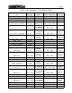
Page 8 Table 3. DC Voltages on Transmitter Board Pin J18 pin 1 (right) J5 pin 5 (bottom) U18 pin 3 (top) Test Point: CWFM Voltage 5.0V VCC 10.0V 9.5V 9.5V Test Point: AM‐ESSB Test Point: SSB JP12 (top) JP12 (bottom) J6 pin 1 (left) JP3 (top) JP4 (top) U20 pin 1 U20 pin 2 U20 pin 4 9.5V 9.5V 5.0V 5.0V 2.5V 2.5V 2.5V 2.5‐3.5V 3.0V 2.
Page 9 Pin Voltage JP7 (left) 1.4V Q3 base (left pin) 1.2V Q3 emitter (right pin) Q3 collector (center pin) 0.4V VCC R21, C9 or C133 (top) Q4 collector (center pin on 2SC1969) Q5 collector (center pin on 2SC1969) 9.5V R42 (top) 5.0V Mode Commands CWUSB, CWLSB, FM Transmitter keyed md3; md7; md4; VCC VCC R42 (top) <0.7V D3 cathode 4.
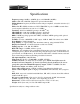
Page 10 Specifications Frequency range: 10 kHz to 30 MHz (Specs valid 500 kHz-30 MHz) Modes: SSB, CW, AM, FM, (Digital via optional embedded PC) FM modulation: frequency modulated carrier with pre-emphasis, selectable deviation (2.5, 4, 5kHz) FM receive IF: 455kHz, includes two ECS LTM455DU 4-pole +/-10KHz ceramic filters (can be replaced with filters as narrow as +/-3KHz) Sensitivity: 0.
Page 11 Theory of Operation The Sienna HF transceiver is organized into five major blocks: • • • • • DC Power conditioning (DCD board) Control (Controller, Front Panel and VFD boards) Receiver (Receiver, BPF and IF Filter boards) Transmitter (Transmitter, TXBPF, Tuner and 100W amplifier boards) PC (PCPS and PC boards) Refer to the Block Diagram on page 43 and the Schematics starting on page 44. DC Power Conditioning: DCD board Over-voltage.
Page 12 motive relay, to open, which removes power. When the comparator outputs are both high, pullup resistor R14 assures that Q2 will be on, enabling the relay to turn on. The relay cannot actually turn on unless the on/off switch is pushed because one side of the relay coil is routed through the switch to DC power. Fuse F1 protects the radio from overcurrent conditions. This is a 9A Resettable fuse.
Page 13 raw input voltage on the audio output amplifiers in order to allow them to handle the very high instantaneous currents (up to an amp!) needed for good speech reproduction. Antenna switch, SWR meter The DCD board also has an antenna A/B switch and an SWR meter on it (see sheet 2 of 3 on the DCD/Tuner schematic). Relay K17 and K18 switch between main antennas A and B. The use of two relays instead of one provides better port-to-port isolation.
Page 14 Control: Controller, Front Panel and VFD Boards The main Controller board is the heart of the Sienna. An Atmel Mega644P microcontroller (U9) running at a clock frequency of 16MHz provides the main control functions, and a second Mega644P (U30) is used for Keyer, VOX/AntiVOX detection, microphone sampling in FM, keypad detection and meter backlight functions.
Page 15 user (the mic’s /PTT) or when the Keyer is controlling it. An output port bit, PTTO, or the Keyer, via PTT_Keyer, are used to generate LTxEn, which is fed to the 10W transmitter as well as the 100W amplifier (Sheet 7). The Keyer microprocessor also controls when the receiver is enabled, through the signal HRcvEn.
Page 16 port C or has been accepted from port C. Q12 provides a Frequency Update pulse for all DDS chips. A4 and A5 are address lines for the DDS chips. Port D has the RS-232C data lines TXD and RXD, Rotary Pulse Generator (RPG) outputs from the two tuning dials, and additional address lines for the internal I/O ports and DDS chips. Sheet 5 shows address decoding for the 16 data strobe lines /Strobe1 though /StrobeG.
Page 17 Note that a similar switch is not needed for the RXVFO, because it operates at a much higher frequency range of 70-100MHz. Any harmonics of 70MHz fall well outside the upper cutoff of the Butterworth bandpass filter (105MHz). LED Backlight Sheet 7 shows backlighting circuitry for the meters. Q13, Q14 and Q15, along with the associated resistors, form a 3-bit binary control, allowing up to 8 brightness levels. The control lines for these MOSFETs come from the Keyer processor.
Page 18 The dot paddle and dash paddle inputs are filtered and fed to two edge-driven interrupt lines (port D, bits 2 and 3). The manual key input is fed to bit 0, where it is sampled continuously in the 1ms interrupt routine. Outputs from the Keyer are the PTT_Keyer line, which is routed to the controller to allow the Keyer to control the PTT line, and the Key line, which is routed to the transmitter. The Keyer processor also has its own SPI bus for programming and a power-on reset chip.
Page 19 (U20/U21 on Sheet 8 of the RXBPF board) is allocated as a bypass. This circuit represents the DZKit exclusive Passive Signal Boost (PSB)TM. By skipping the BPFs, any associated front-end loss is eliminated at the expense of a potential increase in intermod, and an increase in the noise floor, since more spectrum is allowed in. However, on a fading band, that extra 5dB of “gain” (actually “lack of loss”) can spell the difference between hearing and not hearing a weak signal.
Page 20 Receiver second IF The 70MHz 1st IF output of the Darlington driver feeds U8, another TUF-3 mixer, along with LO2 from the controller set to 61.455Mhz (+/-, depending on filters in use and desired sideband). The difference product of about 9MHz is used for the 2nd IF, allowing a wide variety of Inrad crystal filters to be used. Transformer T4 boosts the 50 ohm output impedance of the mixer up to 1800 ohms while providing a factor of 6 voltage gain.
Page 21 tweaked so that the loss through the IF Filter board is about the same regardless of the loss characteristics of the various filters. The crystal filters have various input/output impedances. The Inrad 2311 is about 400 ohms, whereas the others are 200 ohms, so an additional matching transformer is required as well as a different value pad. The IF Filter board is designed to accommodate the filters (except the 2311) on Yaesucompatible plug-in boards.
Page 22 the input offset and input bias current of the op-amp do not add a DC offset to the small AGC voltage. U27 (pins 1,2,3) multiplies the AGC voltage by 17 in a non-inverting configuration, resulting in a 0-1.3V output swing. The other half of U27 level shifts the 0-1.3V signal to 3.755.1V which becomes the AGC voltage that is fed into U9. U10 provides the necessary negative output that sets the differential amplifier offset.
Page 23 This is one thing that enables high speed QSK (full break-in) operation. There’s one other thing that must be done during non-full-duplex transmit. The receiver cannot help but pick up a little of the transmitted signal, and we do not usually want to hear that in the speakers. Therefore the audio output must be muted during transmit. This is done by Q34 (Sheet 8).
Page 24 ers. However it can cause the receiver to have higher pitch than may be comfortable. The solution is to mute the receiver and use the line out to the internal or external PC sound card, and to run the audio through a DSP such as SiliconPixels’ ChromaSound software, which is included when you buy the PC option. Another alternative is to use the graphic equalizer on the sound card to reduce high frequencies.
Page 25 a calculated value and depends on the meter function that is selected (SWR, Forward Power, PA Volts, etc.).
Page 26 Transmitter: Transmitter, TxBPF and 100W PA boards Refer to the block diagram on page xxx and schematics starting on page xxx. The transmitter in the Sienna is completely separate from the receiver. They do not share local oscillators or bandpass filters as is the case in most transceivers. This allows the transmitter and receiver to be operated at the same time, i.e.
Page 27 off. In FM mode, the key is turned on and TXBFO is frequency modulated based on the amplitude of the sampled microphone input. SSB/AM filtering The transformer-coupled (T6) DSB signal from U7 (107A and 107B) is applied to two 7element variable bandwidth Cohn-style crystal filters, one for SSB use, with a 2.5 kHz bandwidth, and one for AM use, with a 5 kHz bandwidth. For SSB use, the LO is shifted above or below the crystal filter’s bandwidth to pick off just the desired sideband.
Page 28 is identical to the ones used on the RXBPF board for the receiver discussed earlier. The only difference is that the TXBPF board selects the band based on 4 bits of band data from U1 (Sheet 8). This band data is compatible with that used by Yaesu’s linear amplifiers. Voltage Controlled Amplifier, ALC The bandpass filtered signal from J13 is next fed into another NXP SA603 voltage controlled amplifier (U8). The BUFALC control voltage (Sheet 9) provides the 2.5V to 3.
Page 29 T/R switch and low pass filters The 10W output from T5 is fed into one of five low pass filters shown on Sheet 7. If the 100W amplifier is not installed, the bandpass filters are also tapped at the 10W signal point and fed through a transmit/receive PIN diode switch network consisting of diodes D3 and D7, chokes RFC1 and RFC2, and output coupling capacitors C80 and C113. Resistors R40 and R42 bias the PIN diodes at half the supply voltage when enabled by Q1.
Page 30 Amp bypass Sheet 2 is the heart of the 100W amplifier. A 10 Watt input signal can either be fed to the amplifier or it can be switched directly to the T/R switch via relays K1 and K2. If the amp is bypassed, the BON signal (derived from the PAON bit before the relay driver on Sheet 1) will stay low, assuring that the amplifier is biased off by U3/Q7.
Page 31 in the secondary is thus about 3 Amps rms. Stability filter and T/R switch RF appearing at K3 is routed to a high pass filter consisting of toroids L14 and L15 and capacitor C70. with a breakpoint at about 1.5MHz. Thus the amplifier cannot be used at full power below this frequency. If the PTT signal is active, the TXPVCC voltage is enabled, and current flows through R23, RFC5, D3, RFC6 and R24, biasing D3 at about 6V and allowing the AC waveform to pass through it via PIN diode action.
Page 32
Page 33 Insert block diagram page here
Page 34 Schematics
Page 35
Page 36
Page 37
Page 38
Page 39
Page 40
Page 41
Page 42
Page 43
Page 44
Page 45
Page 46
Page 47
Page 48
Page 49
Page 50
Page 51
Page 52
Page 53
Page 54
Page 55
Page 56
Page 57
Page 58
Page 59
Page 60
Page 61
Page 62
Page 63
Page 64
Page 65
Page 66
Page 67
Page 68
Page 69
Page 70
Page 71
Page 72
Page 73
Page 74
Page 75
Page 76
Page 77
Page 78
Page 79
Page 80
Page 81
Page 82
Page 83
Page 84
Page 85
Page 86
Page 87
Page 88
Page 89
Page 90
Page 91
Page 92
Page 93
Page 94
Page 95
Page 96
Page 97
Page 98 DZ COMPANY LOVELAND, COLORADO UNIQUE electronic equipment in kit form