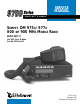
SERVICE MANUAL MULTI-NET ® II MOBILE SUMMIT DM 975X/977X 800 or 900 MHZ MOBILE RADIO ® MULTI-NET® II 13.6 VDC, 15 or 30 Watts Part No.
MULTI-NET® ® SUMMIT DM 975x/977x 800/900 MHz TRUNKED RADIO 13.6 VDC, 15 or 30/35 Watts, FM 806-821 MHz Tx, 851-866 MHz Rx (975x) 896-902 MHz Tx, 935-941 MHz Rx (977x) Part No. 242-97xx-111 Copyright © 2000 by the E.F. Johnson Company The E.F. Johnson Company designs and manufactures two-way radio equipment to serve a wide variety of communication needs. E.F.
TABLE OF CONTENTS TABLE OF CONTENTS 1 GENERAL INFORMATION 3 OPERATION 1.1 1.2 3.1 3.2 1.3 1.4 1.5 1.6 1.7 1.8 1.9 SCOPE OF MANUAL . . . . . . . . . . . . . . . . . . . . 1-1 EQUIPMENT DESCRIPTION . . . . . . . . . . . . . 1-1 General . . . . . . . . . . . . . . . . . . . . . . . . . . . . . . . . 1-1 Programming . . . . . . . . . . . . . . . . . . . . . . . . . . . 1-1 Selectable Systems and Groups . . . . . . . . . . . . . 1-1 Front and Remote Mounting . . . . . . . . . . . . . . .
TABLE OF CONTENTS (CONT’D) Profile . . . . . . . . . . . . . . . . . . . . . . . . . . . . . . . . 3-14 Banks . . . . . . . . . . . . . . . . . . . . . . . . . . . . . . . . 3-14 Power Turn-Off Delay . . . . . . . . . . . . . . . . . . . 3-15 Emergency Calls. . . . . . . . . . . . . . . . . . . . . . . . 3-15 Programmable Power Output . . . . . . . . . . . . . . 3-16 Automatic Transmitter Thermal Foldback . . . . 3-16 Data System/Groups . . . . . . . . . . . . . . . . . . . . . 3-16 Encryption . . . . . . .
TABLE OF CONTENTS (CONT’D) 5.2 5.3 5.4 5.5 5.6 5.7 5.8 Radio Network Terminal (RNT) . . . . . . . . . . . . 5-2 Dispatch Consoles . . . . . . . . . . . . . . . . . . . . . . . 5-2 Public Switched Telephone Network (PSTN) . . 5-2 DEFINITIONS OF MULTI-NET TERMS . . . . 5-3 HOME AND STATUS REPEATERS . . . . . . . 5-4 HOME CHANNEL BACKUP . . . . . . . . . . . . . .5-4 Introduction . . . . . . . . . . . . . . . . . . . . . . . . . . . . 5-4 Selecting Repeater To Monitor . . . . . . . . . . . . .
TABLE OF CONTENTS (CONT’D) Identifying SMD Resistors . . . . . . . . . . . . . . . . . SMD Capacitor Identification . . . . . . . . . . . . . . SMD Inductor Identification . . . . . . . . . . . . . . . Transistor/Diode Identification . . . . . . . . . . . . . 8 8.1 ALIGNMENT PROCEDURE AND PERFORMANCE TESTS RF Board 8.5 8.6 GENERAL. . . . . . . . . . . . . . . . . . . . . . . . . . . . . . 8-1 Introduction . . . . . . . . . . . . . . . . . . . . . . . . . . . . 8-1 Test Cables . . . . . . . . . . . . .
TABLE OF CONTENTS (CONT’D) APPENDIX B UNIVERSAL DIGITAL AND DATA INTERFACE B.1 B.2 B.3 B.4 B.5 B.6 B.7 B.8 4-6 4-7 4-8 4-9 4-10 5-1 6-1 6-2 7-1 8-1 8-2 8-3 8-4 B-1 B-2 B-3 B-4 GENERAL INFORMATION . . . . . . . . . . . . . . B-1 Scope . . . . . . . . . . . . . . . . . . . . . . . . . . . . . . . . . B-1 Universal Interface Description . . . . . . . . . . . . . B-1 POWER SUPPLY . . . . . . . . . . . . . . . . . . . . . . B-2 RECEIVE AUDIO SIGNALS . . . . . . . . . . . . . B-2 Pin Descriptions . . . . .
GENERAL INFORMATION SECTION 1 GENERAL INFORMATION 1.1 SCOPE OF MANUAL programming software listed in Table 1-1. Transceiver operating parameters are stored in an EEPROM reprogrammable memory. Refer to Section 4 for more programming information. This service manual contains installation, operation, programming, alignment, and service information for the E.F. Johnson Summit® DM 975x and 977x transceivers. The operating code (firmware) for the microprocessor is stored in a flash-type memory device.
GENERAL INFORMATION 1.5 ACCESSORIES The remote control unit uses the same front panel assembly that is used on front mount transceivers. Therefore, it operates the same as a front-mount transceiver. A Remote Conversion Kit is available which converts the front panel of a front mount transceiver to a remote control unit (see Table 1-1). The remote control unit has an internal 5-watt speaker or an external 15-watt speaker can be used.
GENERAL INFORMATION Table 1-1 ACCESSORIES Accessory Mounting Accessories [1] Mounting bracket & hardware kit DC power cable & hardware, 22' Accessory cable Key cap kit, Summit Lockable Mounting Tray Adapter cable (to use 86xx-series power cable with 97xx) Part No.
GENERAL INFORMATION Table 1-2 E.F.
GENERAL INFORMATION When your call is answered at the E.F. Johnson Company, you will hear a brief message informing you of numbers that can be entered to reach various departments. This number may be entered during or after the message using a tone-type telephone. If you have a pulse-type telephone, wait until the message is finished and an operator will come on the line to assist you. When you enter some numbers, another number is requested to further categorize the type of information you need.
GENERAL INFORMATION 1.9 REPLACEMENT PARTS charge by calling the repair lab (see Section 1.7) or by requesting them when you send a unit in for repair. Clearly describe the difficulty experienced in the space provided and also note any prior physical damage to the equipment. Then include a form in the shipping container with each unit.
GENERAL INFORMATION SUMMIT® DM 975x (800 MHz) SPECIFICATIONS The following are general specifications intended for use in testing and servicing this transceiver. For current advertised specifications, refer to the specification sheet available from the Marketing Department. Specifications are subject to change without notice.
GENERAL INFORMATION SUMMIT® DM 977x (900 MHz) SPECIFICATIONS The following are general specifications intended for use in testing and servicing this transceiver. For current advertised specifications, refer to the specification sheet available from the Marketing Department. Specifications are subject to change without notice.
INSTALLATION SECTION 2 INSTALLATION Item No. Description Item No. Part No. Description Part No.
INSTALLATION 2.1.3 TRANSCEIVER PROGRAMMING 2.2 TRANSCEIVER INSTALLATION The transceiver needs to be programmed before it is placed in service unless it was ordered as factory programmed. Programming instructions are located in Section 4. Transceivers not factory programmed are shipped programmed with test channels and other factory test parameters. 2.2.1 GENERAL Cable and Hardware Kit, Part No.
INSTALLATION Figure 2-2 Accessory Jack alert, public address, and external emergency switch accessories. then splice it using the included butt splice connectors. You may also need to cut the cable if it must be routed through the firewall and there is no opening large enough to clear the fuseholder. If a hole is drilled in the firewall, be sure to seal it when the installation is complete. Two 8-pin connectors are included.
INSTALLATION 2.4.4 HORN ALERT pin 1 back in to the internal speaker connected to pin 3. The other internal speaker terminal is internally connected to pin 2. The horn alert feature enables the vehicle horn or some other type of alert such as the lights when a call is received that is programmed for this feature. For more operation information, refer to Section 2.4.4. External Speaker With front-mount transceivers, 4-ohm, 15-watt external speaker, Part No.
INSTALLATION Item No. Description Part Number Item No. 1 2 3 4 5 6 7 Amplified dynamic mic Screw, 4-20 x 5/8” thrd frmg (3) Screw, 4-24 x 1/4” sheet metal (3) Microphone hanger clip Mic hanger ground wire Transceiver mounting bracket Self-drilling screw, 1.
INSTALLATION “Disabled” is selected. When “Remote” is selected, the transceiver and control unit volume controls operate in parallel (the volume level is the sum of the levels set by both controls). When “Disabled” is selected, only the transceiver volume control sets the volume level. In the dual control configuration, the levels of the transceiver and control unit internal speakers are the same. program special configurations, refer to the information which follows.
INSTALLATION Figure 2-4 Remote Control Unit Programming Switches c. To change the default backlight condition, press the Select switch so that the backlight is either on or off as desired. Keypad and Knob Disable (S101-1, 2) S101-1 Select Knob Enabled Select Knob Disabled Keypad Enabled Keypad Disabled Off On ----- S101-2 d. To change the LCD viewing angle, rotate the Select switch in either direction to achieve the desired sharpness. ----Off On e.
INSTALLATION (high) state. This is sensed by the microprocessor which may then initiate such actions as halting scanning or enabling the conventional monitor mode. c. Install the microphone hanger in a convenient location using the screws for sheet metal or plastic. The hanger must be connected to chassis ground for proper operation of functions such as monitoring and scan. If required, ground the hanger using the included ground wire.
INSTALLATION 2.7 INSTALLING DC NOISE FILTER KIT The DC Noise Filter Kit is available as a field or factory installed option as described in Section 1.5. This kit contains filter choke, Part No. 542-5010-005, which is installed in the main 13.8-volt line on the PA board. To install this choke, proceed as follows: a. Remove both the red and blue power cable leads from the PC board as shown in Figure 2-5. This provides the needed access to the front of the choke. b.
INSTALLATION 2.8 TRANSCEIVER MOUNTING TRAY INSTALLATION b. Install lock bracket MP1 using the four self-drilling screws (HW3) and washers (HW5) included. Make sure that there is nothing under the mounting location that will be damaged. 2.8.1 DESCRIPTION Optional Transceiver Locking Tray, Part No. 5857000-185, is a lockable mounting bracket for Summit DM transceivers and other transceivers that use that chassis.
OPERATION SECTION 3 OPERATION • • 3.1 FEATURES NOTE: System operator programming determines the availability of some of the preceding features. CONVENTIONAL FEATURES • • • • • • • GENERAL FEATURES • • • • • • • • • • • • • • • • • • • • • Up to 32-100 systems programmable (the maximum varies with type and no.
OPERATION PTT Switch Optional DTMF Microphone Option Switches (6) Display Transmit Indicator Mic Jack On-Off/Volume Select Switch Speaker Figure 3-1 Front Panel Controls Power Jack - Connection point for the 12-volt, negative ground power source. display. In addition, the return time can be programmed for 1-15 seconds or infinite. (The return time is the time that elapses before the bar goes back to the default position.
OPERATION 3.2.2 DISPLAY P1/P2 - When a conventional system is selected, “P1” indicates that a call is being received on a priority 1 group, and “P2” indicates that a call is being received on a priority 2 group. Refer to Section 3.5.17 for more information. Backlight - The display has a backlight which can be programmed to automatically turn on with transceiver power or it can be controlled manually by the BKLHT option switch or Menu Mode “BACKLIGHT” parameter (see Section 3.5.5).
OPERATION 3.3 OPERATING MODES are no tones or display messages to indicate busy and out-of-range conditions. 3.3.1 INTRODUCTION Monitoring Before Transmitting Each selectable system can be programmed with a unique set of transceiver operating parameters. One of these parameters is the operating mode which can be Multi-Net, LTR, or conventional. The type or types of operation programmed is determined by the radio equipment that is being accessed by that system.
OPERATION immediately drops that call and switches to another repeater to receive the higher priority call. Block Up to all 225 (M-Net) Up to all 250 (LTR) ----- The priority order of the receive ID codes is as follows: Groups 1.Fixed Priority ID Code 1 2.Fixed Priority ID Code 2 3.Selectable ID Codes (with last sel revert prog) 4.Block ID codes Each group switch position selects one of the selectable ID codes.
OPERATION Table 3-1 Multi-Net Standard And Special Call Receive Priority Interrupting Call Call in Progress Standard InterconInterroAuxiliary Group nect gate Kill Reassign Emergency All Call Standard Group [1] [1] [1] Yes Yes Yes Yes Yes Interconnect No No No No Yes Yes Yes Yes Auxiliary No No No No No No Yes Yes Interrogate No No No No No No Yes Yes Kill No No No No No No Yes Yes Reassignment No No No No No No Yes Yes Emergency No No No No No No --Yes All Call No No No No No No [2] -[1] With these
OPERATION Receive Delay If LTR or conventional systems are also programmed, they are skipped in the scan sequence because only Multi-Net systems are scanned. If an attempt is made to enter scanning on with an LTR or conventional system displayed, scanning can be selected only if Multi-Net auto-registration is enabled. Auto-registration then occurs and scanning begins on that site. If auto-registration is not programmed, an error tone sounds, “NOT MULTI” is displayed, and the scan mode is not entered.
OPERATION 3.4.6 SCAN LIST PROGRAMMING with a fixed transmit system/group as described in Section 3.4.5. The three programmable configurations are as follows: Systems and groups can be added to or deleted from the scan list if the transceiver is equipped with an A/D (add/delete) option switch. The bar above the system or group indicates which will change when the A/D switch is pressed. To switch this bar between the system and group displays, press the Select switch.
OPERATION Table 3-2 Menu Mode And Option Switch Functions FUNCTION A/D (Scn List Prg) Auto-Registration Auxiliary 1 Auxiliary 2 Backlight Bank Select Call Guard Disable Emergency Encryption Ext PA (Mic audio) Ext PA (Rx audio) Home Sys/Grp Horn/Light Alert MENU OPTION SWITCH ITEM SWITCH LABEL X X X X X X X X X X A/D X X X X X X X X X X X AUX 1 AUX 2 BKLHT BANK CG EMER ENCPT PA-MC PA-RX HOME HORN FUNCTION MENU OPTION SWITCH ITEM SWITCH LABEL LTR System Search Menu Mode Select Monitor Phone Mode Se
OPERATION If the transceiver is equipped with a MENU option switch, the Menu Mode can also be selected to control various functions. The functions that can be controlled by the Menu Mode are indicated in Table 3-2 by an “X” in the “MENU ITEM” column. which is changed. To move this bar between the system and group, press the Select switch. An asterisk in the status display next to the system or group indicates that it is in the scan list. Refer to Section 3.4.6 for more information.
OPERATION 3.5.7 CALL GUARD SQUELCH DISABLE HOME option switch. This function can also be used in the scan mode (scanning halts for the length of the receive scan delay). The CG option switch is used to disable both transmit and receive Call Guard squelch on the selected conventional system/group (if it has been programmed). It does not affect Call Guard squelch operation on other system/groups. The disable mode is indicated by a triangle in the display under the switch. See Section 3.6.
OPERATION 3.5.18 RADIO SOUNDS that condition. Refer to Section 3.7.3 for more information. The Menu Mode “RADIO SNDS” parameter selects the tones that are heard when switches are pressed or busy or out-of-range conditions exist. If this menu item is not enabled, the tones that sound are fixed by system operator programming. The four available conditions are as follows: 3.5.
OPERATION individually enabled or disabled on each dispatch group (a fixed delay of approximately 500 ms occurs with interconnect and auxiliary calls). This feature can be used to delay speaking with calls which have a longer setup time. This delay is available only with transceiver software, Version 222 or later, and programming software, Version 206 or later. vehicle.
OPERATION on) but does not automatically turn back on again when the ignition switch is turned off. Therefore, it must be manually turned on after starting the vehicle. Mode A2 - If the horn alert is to be always enabled when transceiver power is on, this mode could be used. Power Switch - The current horn alert mode does not change when power is turned on and off using the front panel power switch. Mode B - This mode could be used if the ignition switch controls power.
OPERATION The general operation of Emergency Calls is described in Section 5.8.11. The two basic operating modes of the emergency switch are Manual Transmit and Automatic Transmit. Multi-Net systems can be programmed for either type; LTR and conventional systems can be programmed for the manual type only. To initiate changing from one bank to another, the BANK option switch or Menu mode “BANK SELCT” parameter is used.
OPERATION If temperature continues to increase at the 2-watt level to the point where more serious damage could occur (this should seldom happen), the transmitter is disabled, a warning tone sounds, and “NO POWER” is displayed. The transmitter remains disabled until temperature decreases to the first temperature limit. Power output is then produced at the 2-watt level. The temperature limits are fixed in hardware. gency system/group every 10 seconds using access priority 1.
OPERATION The identification could include, for example, up to ten digits of the number being dialed or the name of the person or place being called. group (by dealer programming or the user), the circle/ triangle symbol shown in Figure 3-3 is displayed. If the transceiver has Version 206 or earlier software (see Appendix A), encryption must be enabled to transmit or receive an encrypted call.
OPERATION 3.6.14 DISPLAY OF SOFTWARE VERSION access is completed. When the access is successful, a beep (standard and auxiliary calls) or a dial tone (telephone calls) sounds and the call can then be placed in the normal manner. When transceiver power is turned on, the transceiver software version number and other information is briefly displayed as shown in the following illustration. Currently, all Summit transceivers are Tier 3.
OPERATION 3.7.2 AUTO-REGISTRATION (MULTI-NET) Revert group selection is determined by the programming of the bank “Wide Area Group Tracking” parameter. If this parameter is programmed “Yes”, the revert group does not change (it is the same as it was before registration on the new site occurred). If this parameter is “No”, the revert group is the group that was displayed when that system was last selected. Refer to Section 4.4.6 for more information on proper wide area group tracking programming.
OPERATION • The transceiver can exit a site while receiving a call, register on a new site, and then continue receiving the call on the new site. • A call can be received on a new site before registration occurs. Auxiliary - These calls allow a mobile to communicate with any individual mobile or a group of mobiles at the same site or another Multi-Net site (when several Multi-Net systems form a network).
OPERATION Special Call Authorization Directed Group Call (Current Site) When a mobile is programmed to make Interconnect calls, system authorization is needed before service is available. This authorization is performed by the system operator using the System Management Module of the RNT. This authorization also determines what type of service is available. For example, a mobile may be authorized to dial local numbers only.
OPERATION To make another call attempt, the PTT switch must be released and then pressed again. However, it is a good idea to wait a few seconds because the 5second timer does not count down while the PTT switch is pressed. It is not possible to complete the call by keeping the PTT switch pressed with the intercept tone sounding. Landside-Originate Special Calls Calls can be also be made from any landside telephone to specific mobiles (Interconnect calls) or groups (Directed Group calls).
OPERATION 3.8 LTR MODE FEATURES and a dial tone sounds. If the number is not dialed within a few seconds, normal operation resumes. This mode can be canceled at any time by activating any user control. 3.8.1 FREE SYSTEM RINGBACK If a busy condition exists when making an LTR telephone call, the Free System Ringback feature automatically signals when the system is no longer busy.
OPERATION 3.9.2 CALL GUARD SQUELCH each second. When the data is decoded, 23-bit samples are taken and then the bits are rotated to determine if a valid code was received. Tone (CTCSS), digital, or inverted digital Call Guard squelch can be programmed on each conventional transmit and receive group in any order desired.
OPERATION detected on the first priority group but is detected on the second priority group if is programmed. If the PRI option switch or the Menu mode “PRIORITY” parameter is available (see Section 3.5.17), priority sampling can be turned on and off. disabled at the system level). Talk-around is then enabled by simply selecting one of those groups. The unique identification can be used to identify which groups are programmed with this feature.
OPERATION number of the system and then when the system answers, a number specifying the mobile being called. This tone sounds to indicate when the number of the mobile should be entered. access attempts are then made until the push-to-talk switch is released and then pressed again.
OPERATION AUTO REG - Indicates that the transceiver is attempting to register on another system. Refer to “Auto-Registration” description on Section 3.7.2. NO TALK - Indicates that talk-around has been disabled on the selected conventional system by programming (refer to Section 3.9.4). BLOCK CALL - Indicates that the call is being received on a Multi-Net or LTR block ID code (refer to Section 3.3.4).
OPERATION The various test functions are selected by pressing or rotating the front panel Select switch. The display indicates the mode that is currently selected and also such things as the selected frequency, power level, or operating mode. While in the test mode, the front panel option switches function as follows: SNGLE SCAN - Indicates that the single-site type of scanning is occurring (refer to Section 3.4.2.
OPERATION 800 MHz TEST FREQUENCIES Prog Ch No. Rx Freq 900 MHz TEST FREQUENCIES Tx Freq Prog Ch No. Block 0 001 381 920 004 [TA] 379 [TA] 918 [TA] 851.0125 MHz 860.5125 MHz 869.9875 MHz 851.0875 MHz 860.4625 MHz 869.9625 MHz 851.0625 MHz 860.3125 MHz 869.7750 MHz 851.1625 MHz 860.3625 MHz 869.8875 MHz 806.0125 MHz 815.5125 MHz 824.9875 MHz 851.0875 MHz 860.4625 MHz 869.9625 MHz 001 240 479 006 [TA] 246 [TA] 473 [TA] 851.2125 MHz 860.5625 MHz 869.8000 MHz 851.2625 MHz 860.4125 MHz 869.
OPERATION (see Section 8). The 2W setting can also be in this range or 1-2 watts. Microphone audio, data, and the receiver are all disabled by this function. Power is adjusted by rotating the Select switch with the PTT switch pressed. The display indicates the relative set point from 0-127 (127 is maximum power). 3.11.6 MODULATION BALANCE The BAL ADJUST function is used to set modulation balance over the entire standard and talk-around frequency bands.
TRANSCEIVER PROGRAMMING SECTION 4 TRANSCEIVER PROGRAMMING Remote Programming Interface (RPI) Cable Part No. 023-9800-000 Part No. 023-9750-005 To Battery To Antenna To Ign Sense Figure 4-1 Programming Setup 4.1 GENERAL The cables from the RPI to the computer and transceiver are not included with the RPI. The 9800 RPI has a female DB9 connector for the computer connection. Since most computers have a male DB9 or DB25 connector, a male DB9 to female DB9 or DB25 cable is usually required.
TRANSCEIVER PROGRAMMING With Summit DM and Viking® HT/GT transceivers, the switch on the RPI selects either the standard or Flash programming mode. The indicator is green when the standard mode is selected and red when the Flash mode is selected. Version 204 - Became available in early 1996. This version has an additional parameter on the “Main Radio Parameters” screen for specifying the horn alert operating mode (see Section 3.6.4). 4.1.4 EEPROM DATA STORAGE Version 205 - Became available mid 1997.
TRANSCEIVER PROGRAMMING 4.1.11 HEADER INFORMATION To unpack these files so that they can be used, first make sure that the current directory is destination directory for these files. For example, if hard drive C: is the destination, make it the current directory (if required) by typing C: (Enter). Then if using a subdirectory, type CD as just described. Then insert the program disk in the computer and type A:SUMMIT2 (or B:SUMMIT2 if drive B: is being used).
TRANSCEIVER PROGRAMMING Figure 4-2 Programming Software Menu Structure 4-4 Revised December 2000 Part No.
TRANSCEIVER PROGRAMMING F2 (Help Screen) - Displays help information on the displayed screen. F3, F8 - Not used. F4 - F6 - Use varies according to the screen that is selected. Refer to the separate screen descriptions for more information. F7 - When in the main menu, displays the serial number of the transceiver being programmed (see next section). F9 (Prev Menu) - Returns to the previous menu or screen. Figure 4-3 Main Menu F10 (Exit Program) - Exits the program and returns to the operating system.
TRANSCEIVER PROGRAMMING ously loaded from disk as described in the preceding section or from a transceiver as described in the next section. If there is no file currently in memory, a message is displayed. This function displays the Modify Radio File menu described in Section 4.3. When the program is started, the last file edited is automatically loaded if it is in the current directory. 4.2.
TRANSCEIVER PROGRAMMING Number/Letters Preceding The Parameter - An alternate method for quickly selecting these screens is to press the number or letter key preceding the description. For example, to select the Setup Menu screen, press “3”. tory are listed and then the arrow and Return keys are used to select the file. When copying a file, it must be given a new name and/or destination in the destination box. The screen displayed by this function follows.
TRANSCEIVER PROGRAMMING An on-off indicator is available in the display for only the first three keys. Since some functions require this indicator, they are not displayed for the keys that do not have an indicator. Refer to Section 3.5 for more information on the option switches. edited is selected from a list of the current systems that is displayed. The arrow and Return keys are used to select the desired system.
TRANSCEIVER PROGRAMMING Figure 4-5 Define Option Buttons Screen Figure 4-6 Setup Menu Functions Screen 4-9 Revised December 2000 Part No.
TRANSCEIVER PROGRAMMING 4.3.6 CREATE/EDIT/COPY/DELETE BANK Create Bank This Create Bank function is used to create a new bank. At least one bank must be created even if banks are not going to be selected. Banks are identified by alpha tag and selected by the BANK option switch or “Bank Select” Menu Mode parameter. An alpha tag can have up to ten characters. Most printable ASCII characters can be used except the following: PTT Tone Delay Programming Screen # & ( ) , .
TRANSCEIVER PROGRAMMING 4.3.8 EDITING UNIQUE ID CODES System programming screen (see Section 4.3.5) or the Create/Edit Bank screen. The unique ID code programmed for each MultiNet system can be edited by selecting the “Setup/ Change Unique ID” parameter in the Modify Radio File menu (see Figure 4-4). This displays the screen shown in Figure 4-8. This screen allows all Multi-Net unique ID's to be conveniently edited without having to display each system screen.
TRANSCEIVER PROGRAMMING priority number being transmitted is greater than the priority number assigned to the ID code being transmitted, the system cannot be accessed at that time. There are various schemes that the repeater may use to determine the current system priority. Refer to the setup section of the repeater service manual for more information. With LTR systems, they can also be assigned arbitrarily.
TRANSCEIVER PROGRAMMING 4.4.6 WIDE AREA GROUP TRACKING PROGRAMMING 4.5 PROGRAMMING ONE TRANSCEIVER WITH ANOTHER (CLONING) When Wide Area Group Tracking is enabled with Multi-Net Auto-Registration (see Section 3.7.2), the same group remains selected when auto-registration on another system occurs. This allows a companion group to be automatically selected in the new system.
TRANSCEIVER PROGRAMMING 023-9750-000 or 023-9800-000, can be used (the earlier 023-5810-000 model will not work). or have questions about accessing the ACES system, call 800-328-3911, extension 7 (USA and Canada) or 507-835-6222, extension 2100 (international). NOTE: The RPI must always be connected to the front panel jack of the transceiver (it cannot be connected to the microphone jack of a remote control unit). 4.6.
TRANSCEIVER PROGRAMMING Audio Circuit States Audio_Rx - Modes 1*, 2, 3, 4 Audio_Tx - Modes 1*, 2, 3, 4 can be programmed and configurations that can be selected for each are described in the following information. Since the specific configuration of these parameters is determined by the equipment being used, detailed programming instructions are not included in this manual (this information should be provided by the equipment manufacturer).
TRANSCEIVER PROGRAMMING SYSTEM PARAMETERS Audio Circuit States Audio_Rx - Modes 1-4, Undefined* Audio_Tx - Modes 1-4, Undefined* * Default condition. If “Undefined” is selected, the radio-level parameter programmed in the preceding section is in effect. Figure 4-10 System Universal Interface Screen 4.7.4 AUXILIARY AND EMERGENCY SWITCH PROGRAMMING When the Auxiliary 2 function is programmed, it uses the OUTPUT B line of the universal interface (see Section 3.5.4).
TRANSCEIVER PROGRAMMING Table 4-1 Main Radio Parameters Screen Parameter Receive Delay Time Call Delay Time Scan Continue Time Acceptable Responses 0, 1, 2, 3, 4, 5, 6, or 7 seconds 0, 1, 2, 3, 4, 5, 6, or 7 seconds 0-60 seconds Description Time before scanning resumes after a message is received (Section 3.4.3). Time before scanning resumes after message is transmitted (Section 3.4.3). Maximum time that a call is monitored before scanning resumes (Section 3.4.3).
TRANSCEIVER PROGRAMMING Table 4-1 Main Radio Parameters Screen (Continued) Parameter Select Knob Return Time Remote Trunk Mount Radio Has Encryption Installed Horn Honk Mode Radio Can Be Disabled (MN Only) Radio Can Be Interrogated (MN Only) Status Definitions Dispatch Tx Camp-On Acceptable Responses Description 0-15 seconds in 1-sec steps Programs the delay after a change is made before the bar returns to the default display programmed above. “0” programs no return.
TRANSCEIVER PROGRAMMING Table 4-2 Multi-Net System Parameters (Continued) Parameter Offset Acceptable Responses Description Yes, No Programs if channels are offset 12.5 kHz on the low side. This applies to channels 1-600 only (Section 4.4.2). Home Repeater 1-30 Programs the number of the home repeater of the transceiver (Section Number 4.4.1). Home Repeater 1-920 (800 MHz) Programs the channel number of the home repeater (Section 4.4.2).
TRANSCEIVER PROGRAMMING Table 4-2 Multi-Net System Parameters (Continued) MULTI-NET GROUP PARAMETERS (The Group Parameter screen is selected by pressing F6) Parameter Asn Alpha Tag Acceptable Responses Description Yes, No A-Z, 0-9, etc. Specifies if the group will be selectable. Specifies the 10-character alpha tag that is displayed when the group is selected. Group Enc/Dec 1-225, 236, 237 [1] Specifies the encode (transmit) and decode (receive) ID codes for that selectable group.
TRANSCEIVER PROGRAMMING Table 4-3 LTR System Parameters Parameter Alpha Tag Acceptable Responses Description Any keyboard character Changes the 10-character alpha tag for the selected system. The system alpha tag is used only for programming and is not displayed by the transceiver. Home Repeater 1-20 Programs the number of the home repeater of the transceiver (Section 4.4.1). Area 0, 1 Selects the area of the LTR system.
TRANSCEIVER PROGRAMMING Table 4-3 LTR System Parameters (Continued) Parameter Acceptable Responses Horn Yes, No Encrypt Yes, No Asn Alpha Tag Group Enc/Dec Call Light Horn Encrypt Scan List Transpond Data Repeater Channel Number (Chn) Ofst (Offset) RIC Description Programs if the horn sounds when a call is received on that ID code (Section 3.6.4). Programs if encryption is used on calls received on that ID code (Section 3.6.12).
TRANSCEIVER PROGRAMMING Table 4-4 Conventional System Parameters Parameter Alpha Tag Acceptable Responses Description Any keyboard character Changes the 10-character alpha tag for the selected system. The system alpha tag is used only for programming and is not displayed by the transceiver. Channel Number 1-920 (800 MHz) Programs the channel number of that system. Channel numbers are shown 1-479 (900 MHz) in the table at the end of this section. Offset Yes, No Programs if the channel is offset 12.
TRANSCEIVER PROGRAMMING Table 4-4 Conventional System Parameters (Continued) CONVENTIONAL GROUP PARAMETERS (The Group Parameter screen is selected by pressing F6) Parameter Asn Alpha Tag Acceptable Responses Description Yes, No A-Z, 0-9, etc. Specifies if the group will be selectable. Specifies the 10-character alpha tag that is displayed when the group is selected. Tx CG None, CG, DCG, IDCG, Programs the type of transmit Call Guard squelch for the indicated group EXT (Section 3.6.2).
TRANSCEIVER PROGRAMMING Table 4-4 Conventional System Parameters (Continued) Parameter Acceptable Responses Scan List Yes, No Data Yes, No Description Programs if that group is scanned by the group scan feature (Section 3.4.7). Programs if that group can be used for data transmissions (Section 3.6.11) Table 4-5 Create/Edit Bank Screen Parameters Parameter Acceptable Responses Alpha Tag A-Z, 0-9, etc.
TRANSCEIVER PROGRAMMING Table 4-5 Create/Edit Bank Screen Parameters (Continued) Parameter Data System/Group Scan Type Wide Area Group Tracking (MN only) Start At Home Acceptable Responses Description Any system/group in Programs the default system/group that is selected for a data transmission selected bank if the selected group is not programmed for data (Section 3.6.11). Multi-Site or Single-Site Programs the type of scanning that occurs when the scan mode is selected (Section 3.4.2).
800 MHz CHANNEL TABLE Prog Chan. FCC Chan. No. No. 1 2 3 4 5 6 7 8 9 10 11 12 13 14 15 16 17 18 19 20 21 22 23 24 25 26 27 28 29 30 31 32 33 34 35 36 37 38 39 40 41 42 43 44 45 46 47 48 49 50 51 52 53 54 1 2 3 4 5 6 7 8 9 10 11 12 13 14 15 16 17 18 19 20 21 22 23 24 25 26 27 28 29 30 31 32 33 34 35 36 37 38 39 40 41 42 43 44 45 46 47 48 49 50 51 52 53 54 Mobile Rx Freq. Mobile Tx Freq 851.0125 851.0375 851.0625 851.0875 851.1125 851.1375 851.1625 851.1875 851.2125 851.2375 851.2625 851.2875 851.
800 MHz CHANNEL TABLE Prog Chan. FCC Chan. No. No. 109 110 111 112 113 114 115 116 117 118 119 120 121 122 123 124 125 126 127 128 129 130 131 132 133 134 135 136 137 138 139 140 141 142 143 144 145 146 147 148 149 150 151 152 153 154 155 156 157 158 159 160 161 162 109 110 111 112 113 114 115 116 117 118 119 120 121 122 123 124 125 126 127 128 129 130 131 132 133 134 135 136 137 138 139 140 141 142 143 144 145 146 147 148 149 150 151 152 153 154 155 156 157 158 159 160 161 162 Mobile Rx Freq.
800 MHz CHANNEL TABLE Prog Chan. FCC Chan. No. No. 217 218 219 220 221 222 223 224 225 226 227 228 229 230 231 232 233 234 235 236 237 238 239 240 241 242 243 244 245 246 247 248 249 250 251 252 253 254 255 256 257 258 259 260 261 262 263 264 265 266 267 268 269 270 217 218 219 220 221 222 223 224 225 226 227 228 229 230 231 232 233 234 235 236 237 238 239 240 241 242 243 244 245 246 247 248 249 250 251 252 253 254 255 256 257 258 259 260 261 262 263 264 265 266 267 268 269 270 Mobile Rx Freq.
800 MHz CHANNEL TABLE Prog Chan. FCC Chan. No. No. 325 326 327 328 329 330 331 332 333 334 335 336 337 338 339 340 341 342 343 344 345 346 347 348 349 350 351 352 353 354 355 356 357 358 359 360 361 362 363 364 365 366 367 368 369 370 371 372 373 374 375 376 377 378 325 326 327 328 329 330 331 332 333 334 335 336 337 338 339 340 341 342 343 344 345 346 347 348 349 350 351 352 353 354 355 356 357 358 359 360 361 362 363 364 365 366 367 368 369 370 371 372 373 374 375 376 377 378 Mobile Rx Freq.
800 MHz CHANNEL TABLE Prog Chan. FCC Chan. No. No. 433 434 435 436 437 438 439 440 441 442 443 444 445 446 447 448 449 450 451 452 453 454 455 456 457 458 459 460 461 462 463 464 465 466 467 468 469 470 471 472 473 474 475 476 477 478 479 480 481 482 483 484 485 486 433 434 435 436 437 438 439 440 441 442 443 444 445 446 447 448 449 450 451 452 453 454 455 456 457 458 459 460 461 462 463 464 465 466 467 468 469 470 471 472 473 474 475 476 477 478 479 480 481 482 483 484 485 486 Mobile Rx Freq.
800 MHz CHANNEL TABLE Prog Chan. FCC Chan. No. No. 541 542 543 544 545 546 547 548 549 550 551 552 553 554 555 556 557 558 559 560 561 562 563 564 565 566 567 568 569 570 571 572 573 574 575 576 577 578 579 580 581 582 583 584 585 586 587 588 589 590 591 592 593 594 541 542 543 544 545 546 547 548 549 550 551 552 553 554 555 556 557 558 559 560 561 562 563 564 565 566 567 568 569 570 571 572 573 574 575 576 577 578 579 580 581 582 583 584 585 586 587 588 589 590 591 592 593 594 Mobile Rx Freq.
800 MHz CHANNEL TABLE Prog Chan. FCC Chan. No. No. 649 650 651 652 653 654 655 656 657 658 659 660 661 662 663 664 665 666 667 668 669 670 671 672 673 674 675 676 677 678 679 680 681 682 683 684 685 686 687 688 689 690 691 692 693 694 695 696 697 698 699 700 701 702 645 646 647 648 649 650 651 652 653 654 655 656 657 658 659 660 661 662 663 664 665 666 667 668 669 670 671 672 673 674 675 676 677 678 679 680 681 682 683 684 685 686 687 688 689 690 691 692 693 694 695 696 Mobile Rx Freq.
800 MHz CHANNEL TABLE Prog Chan. FCC Chan. No. No. 757 758 759 760 761 762 763 764 765 766 767 768 769 770 771 772 773 774 775 776 777 778 779 780 781 782 783 784 785 786 787 788 789 790 791 792 793 794 795 796 797 798 799 800 801 802 803 804 805 806 807 808 809 810 749 750 751 752 753 754 755 756 757 758 759 760 761 762 763 764 765 766 767 768 769 770 771 772 773 774 775 776 777 778 779 780 781 782 783 784 785 786 787 788 789 790 791 792 793 794 795 796 797 798 799 800 Mobile Rx Freq.
800 MHz CHANNEL TABLE Prog Chan. FCC Chan. No. No. 865 866 867 868 869 870 871 872 873 874 875 876 877 878 879 880 881 882 883 884 885 886 887 888 889 890 891 892 - Mobile Rx Freq. Mobile Tx Freq 869.3000 869.3125 869.3250 869.3375 869.3500 869.3625 869.3750 869.3875 869.4000 869.4125 869.4250 869.4375 869.4500 869.4625 869.4750 869.4875 869.5000 869.5125 869.5250 869.5375 869.5500 869.5625 869.5750 869.5875 869.6000 869.6125 869.6250 869.6375 824.3000 824.3125 824.3250 824.3375 824.3500 824.3625 824.
900 MHz CHANNEL TABLE Prog Chan. FCC Chan. No. No. 1 2 3 4 5 6 7 8 9 10 11 12 13 14 15 16 17 18 19 20 21 22 23 24 25 26 27 28 29 30 31 32 33 34 35 36 37 38 39 40 41 42 43 44 45 46 47 48 49 50 51 52 53 54 1 2 3 4 5 6 7 8 9 10 11 12 13 14 15 16 17 18 19 20 21 22 23 24 25 26 27 28 29 30 31 32 33 34 35 36 37 38 39 40 41 42 43 44 45 46 47 48 49 50 51 52 53 54 Mobile Rx Freq. Mobile Tx Freq 935.0125 935.0250 935.0375 935.0500 935.0625 935.0750 935.0875 935.1000 935.1125 935.1250 935.1375 935.1500 935.
900 MHz CHANNEL TABLE Prog Chan. FCC Chan. No. No. 109 110 111 112 113 114 115 116 117 118 119 120 121 122 123 124 125 126 127 128 129 130 131 132 133 134 135 136 137 138 139 140 141 142 143 144 145 146 147 148 149 150 151 152 153 154 155 156 157 158 159 160 161 162 109 110 111 112 113 114 115 116 117 118 119 120 121 122 123 124 125 126 127 128 129 130 131 132 133 134 135 136 137 138 139 140 141 142 143 144 145 146 147 148 149 150 151 152 153 154 155 156 157 158 159 160 161 162 Mobile Rx Freq.
900 MHz CHANNEL TABLE Prog Chan. FCC Chan. No. No. 217 218 219 220 221 222 223 224 225 226 227 228 229 230 231 232 233 234 235 236 237 238 239 240 241 242 243 244 245 246 247 248 249 250 251 252 253 254 255 256 257 258 259 260 261 262 263 264 265 266 267 268 269 270 217 218 219 220 221 222 223 224 225 226 227 228 229 230 231 232 233 234 235 236 237 238 239 240 241 242 243 244 245 246 247 248 249 250 251 252 253 254 255 256 257 258 259 260 261 262 263 264 265 266 267 268 269 270 Mobile Rx Freq.
900 MHz CHANNEL TABLE Prog Chan. FCC Chan. No. No. 325 326 327 328 329 330 331 332 333 334 335 336 337 338 339 340 341 342 343 344 345 346 347 348 349 350 351 352 353 354 355 356 357 358 359 360 361 362 363 364 365 366 367 368 369 370 371 372 373 374 375 376 377 378 325 326 327 328 329 330 331 332 333 334 335 336 337 338 339 340 341 342 343 344 345 346 347 348 349 350 351 352 353 354 355 356 357 358 359 360 361 362 363 364 365 366 367 368 369 370 371 372 373 374 375 376 377 378 Mobile Rx Freq.
900 MHz CHANNEL TABLE Prog Chan. FCC Chan. No. No. 433 434 435 436 437 438 439 440 441 442 443 444 445 446 447 448 449 450 451 452 453 454 455 456 433 434 435 436 437 438 439 440 441 442 443 444 445 446 447 448 449 450 451 452 453 454 455 456 Mobile Rx Freq. Mobile Tx Freq 940.4125 940.4250 940.4375 940.4500 940.4625 940.4750 940.4875 940.5000 940.5125 940.5250 940.5375 940.5500 940.5625 940.5750 940.5875 940.6000 940.6125 940.6250 940.6375 940.6500 940.6625 940.6750 940.6875 940.7000 901.4125 901.
MULTI-NET SYSTEM OVERVIEW SECTION 5 MULTI-NET SYSTEM OVERVIEW REPEATERS (UP TO 30 PER RNT) OTHER RNT'S AND SYSTEMS AUDIO AND DATA LINK MULTI-NET 856x/7x/8x/9x, 8605/15/22/55, RADIO NETWORK TERMINAL (RNT) SUMMIT DM 975x/977x MOBILE TRANSCEIVERS MULTI-NET PUBLIC SWITCHED TELEPHONE NETWORK (PSTN) AUDIO AND DATA LINK LTR 98xx, 8600/04, 856x/857x, 5876, 86xx, VIKING GT/HT 965x/967x MOBILE TRANSCEIVERS LTR DISPATCHER CONSOLE AUDIO AND DATA LINK CONVENTIONAL 98xx, 5876, 71x6/718x CONVENTIONAL SYSTEM M
MULTI-NET SYSTEM OVERVIEW 5.1.4 RADIO NETWORK TERMINAL (RNT) or another Multi-Net system. Phone lines or some other type of link can be used to provide a communication path. The RNT along with the SMM (System Management Module) control the Multi-Net system. The SMM is an IBM® PC or compatible computer that is running Multi-Net software. This computer connects to the RNT and is used by the system manager to control the system.
MULTI-NET SYSTEM OVERVIEW 5.2 DEFINITIONS OF MULTI-NET TERMS Radio Network Terminal (RNT) - The RNT together with the System Management Module provide control of a Multi-Net system. The RNT can interconnect several different forms of communication to form a communication network. Refer to Section 5.1.4 for more information. Conventional System - A type of radio system that is licensed to operate on only a single channel. There is no automatic access to several channels.
MULTI-NET SYSTEM OVERVIEW 5.3 HOME AND STATUS REPEATERS repeater became inoperative, all the mobiles assigned to that home repeater would not be able to place or receive calls. To prevent this from happening, each site utilizing Multi-Net signaling has a repeater called a status repeater which transmits update messages for all calls occurring at the site. All mobiles assigned to the site can receive update messages from either the status or home repeater.
MULTI-NET SYSTEM OVERVIEW If it is a home repeater, these messages are for its assigned mobiles that are being trunked to other repeaters. If it is the status repeater, messages to all mobiles currently using the site are transmitted. If it has assigned mobiles, this includes messages to those mobiles. For example, assume that five different transceivers are making calls. If all have Repeater 1 as their home repeater, the data message order on Repeater 1 is as follows: 1 2 3 1 4 5 1 2 3 and so on.
MULTI-NET SYSTEM OVERVIEW 5.8 OTHER MULTI-NET FEATURES With Multi-Net signaling, repeater data bus synchronization is done distributively. Therefore, no single repeater is responsible for data bus synchronization. If any of the repeaters at the site become inoperative, the others continue to operate normally. 5.8.1 UNIQUE ID CODES Each selectable system of a transceiver is programmed with a unique ID code in addition to the group ID codes.
MULTI-NET SYSTEM OVERVIEW Telephone and other special calls cannot be interrupted by standard calls. Refer to Section 3.7.4 for more information. group reprogrammable in this manner prevents the transceiver from becoming inoperative because of a programming error caused by a poor RF signal. 5.8.3 ALL CALL Dynamic reprogramming is performed by the system manager.
MULTI-NET SYSTEM OVERVIEW Most Multi-Net transceivers also have a programmable parameter called Auto-Registration Dropout Criteria. This parameter determines the point at which the mobile attempts to register on another site. This is controlled by the percentage of good data messages that the mobile receives over a 10-second period. If it is programmable, it can be set for 50-100%. If it is not, it is fixed at 50%.
MULTI-NET SYSTEM OVERVIEW 5.8.16 VOICE ENCRYPTION Encryption can be used with Multi-Net, LTR, and conventional operation. Each group can be programmed for encryption and then when that group is selected, encryption is automatically enabled. The user can also manually turn encryption on and off. The encryption mode is indicated in the display or by a front-panel indicator. NOTE: Voice encryption is currently not available for E.F. Johnson 900 MHz transceivers.
MULTI-NET SYSTEM OVERVIEW 5-10 Revised February 1997 Part No.
CIRCUIT DESCRIPTION SECTION 6 CIRCUIT DESCRIPTION 6.1 GENERAL TRANSCEIVER DESCRIPTION 6.1.3 RECEIVER 6.1.1 INTRODUCTION The receiver is a double-conversion type with intermediate frequencies of 52.950 MHz and 450 kHz. Receiver selectivity is enhanced by two 52.950 MHz crystal filters and a 450 kHz ceramic filter. Two bandpass filters in the front end attenuate the image, half IF, injection, and other frequencies which could degrade receiver performance.
CIRCUIT DESCRIPTION transmit frequency in the transmit mode and 52.950 MHz below the receive frequency in the receive mode. Therefore, its operating band is approximately 798869 MHz (800 MHz models) or 882-941 MHz (900 MHz models). Transistor bias is provided by R920 and R921, and stabilization is provided by R922. L921 is an RF choke and C926 is a bypass capacitor. C922, C923, and R924 provide feedback to start and maintain oscillation and also match the oscillator to the tank circuit.
CIRCUIT DESCRIPTION Figure 6-1 Transceiver Block Diagram 6-3 August 1993 Part No.
CIRCUIT DESCRIPTION The capacitive leg is formed by C905, PIN diode CR905, and C906. When the Q6 output of U802 is a high level and the Q7 output is a low level, CR905 is forward biased and C905 and C906 are effectively connected to the tank circuit. This decreases the resonant frequency of the tank circuit. L905/L906 and C907/C908 provide isolation. The inductive leg is formed by C909, a section of microstrip (which provides series inductance), and by C910.
CIRCUIT DESCRIPTION Figure 6-2 U801 Block Diagram receiver, and CR902 presents a high-impedance into the transmitter. L800/C841 and L803/C813 neutralize the slight capacitance of the diode when it is reverse biased to improve isolation. remains stable over changes in temperature. flows so that the voltage drop across R809 equals the drop across R815 and the base- emitter junction of Q802.
CIRCUIT DESCRIPTION counter reaches zero. Both counters then reset and the cycle is repeated. The A counter is always programmed with a smaller number than the N counter. While the A counter is counting down, the modulus control output to the prescaler (pin 12) is low and the prescaler divides by 129. Then when the A counter is halted, the modulus control output is high and the prescaler divides by 128. programming circuitry. The basic operation was described in Section 6.2.1.
CIRCUIT DESCRIPTION 6.2.9 VOLTAGE MULTIPLIER (CR804A/B, CR805A/B) This lock detect signal is integrated by Q808 and Q809. C831 charges through R830 and R832 and discharges through C831 and Q808. When the negative-going lock detect pulses widen, C831 discharges to the turn-off point of Q809. The collector of Q809 then goes high and this signal is applied to the 5D pin of input latch U411 on the audio/logic board.
CIRCUIT DESCRIPTION biased so that the voltage drop across R297 is equal to the drop across R294 and the base- emitter of Q291. This arrangement provides a bias that remains stable as changes occur in temperature. in Section 6.3.1. The output of the IF amplifier is applied to a 6 dB pad and then to crystal filter Z206. This is a two-pole filter with a bandwidth of 18 kHz (800 MHz) or 10 kHz (900 MHz) at the –3 dB points.
CIRCUIT DESCRIPTION 6.4 TRANSMITTER CIRCUIT DESCRIPTION Pin 10 of U200 is the output of an internal RSSI (receive signal strength indicator) circuit. It provides a high-impedance current sink that increases in conduction in proportion to increases in the IF signal level. The result is that the voltage on pin 10 decreases as the IF signal strength increases and vice versa. This signal is buffered by U201B and then fed to comparator U602C on the audio/logic board.
CIRCUIT DESCRIPTION power levels that can be programmed using the test mode (see Section 3.11). Power output is controlled by varying the supply voltage to one of the amplifier stages in power amplifier module U500. The microprocessor also monitors transmitter temperature and if it is not in the normal range, power is automatically cut back to prevent damage. In the transmit mode, Q507 and Q514 are turned on.
CIRCUIT DESCRIPTION amplifier U504D. The base voltage of Q502 is controlled by current sense amplifier Q506 and a D-A converter formed by shift register U503 and a resistor network. the data bus (AD0-AD7) to be used for memory addressing as well as data input and output. For more information, see “Address/Data Bus” description which follows. As the voltage from the D-A converter increases, Q502 and Q511 turn on more which causes power output to increase.
CIRCUIT DESCRIPTION This voltage decreases as power amplifier temperature increases. drops below the normal range. Reset clears several internal registers and restarts the operating program. This prevents improper operation resulting from lowvoltage conditions. PE1 - Analog DC voltage of 0-5 volts from the directional coupler on the PA board that increases with the reflected power. This and the PE2 input are currently not used.
CIRCUIT DESCRIPTION the digital signal processor circuit in the slave configuration. Serial RS-232 Interface The serial RS-232 port has three functions. First, it provides data communication with the computer used to program the transceiver. Connection is made via the microphone connector on either the front panel or remote control unit. PD5 (SS) - In the slave configuration, this is the slave select input and the master forces it low when it is ready to transfer data.
CIRCUIT DESCRIPTION U406. This prevents inadvertent writing to that device. The F7 output of U407 is not used. pin 2. If the RX LOOP signal is high, the opposite occurs. 6.5.3 DIGITAL SIGNAL PROCESSOR (U300U302) R644, R645, and C639 are used to minimize the “click” heard when the gate opens and closes. R625 and C638 attenuate noise present in the logic signal. Diode CR601 closes both U608A and U608C whenever mute gate U608B is closed. This improves isolation.
CIRCUIT DESCRIPTION This channel of U600 is normally not used with front-mount transceivers and is programmed for maximum attenuation because the PE4 input is pulled low by R785. An exception may be when a remote control unit is used with a front-mount transceiver to provide dual controls. The volume controls of both units can then operate in parallel so that the volume is the sum of both controls (see Section 2.5.1). The second channel of U600 is not used at this time.
CIRCUIT DESCRIPTION valid data may be present. The squelch circuit is controlled by the amount of noise present in the receive audio signal. When no signal or a weak signal is being received by the receiver, there is a large amount of noise present. Conversely, when a strong signal is being received, there is very little noise present. If the remote control unit is used, a 600-ohm balanced line is used to apply the audio signal to differential amplifier U603A.
CIRCUIT DESCRIPTION provided by R708 and R709. The output of the summing amplifier is fed to the synthesizer on the RF board. If optional companding is used, jumper R690 is removed and the compandor board is installed. Companding is the compressing and then expanding of the audio signal to reduce noise. This also increases the dynamic range of the audio signal which is otherwise limited by channel spacing.
CIRCUIT DESCRIPTION 6-18 August 1993 Part No.
SERVICING SECTION 7 SERVICING 7.1 GENERAL mode is especially useful when the transceiver is programmed for LTR operation because the logic inhibits operation until a handshake is completed with a repeater. 7.1.1 PERIODIC CHECKS This transceiver should be put on a regular maintenance schedule to ensure that it continues to operate properly. Important checks are receiver sensitivity and transmitter frequency, deviation, and power output.
SERVICING Once the device is installed in the PC board, it is protected by internal diode protection circuits, so the chance of damage is reduced. A service bench protection kit, Part No. 299-0026-001, can be ordered from the Service Parts Department. This kit includes a conductive mat, wrist strap, and grounding strap with a 1 megohm resistor to eliminate static build-up on the body. 7.2.3 VCO MODULE AND PRESCALER 7.
SERVICING Figure 7-1 Simplified Synthesizer Block Diagram channel you have selected is calculated as described in Section 7.2.5. The input and output frequencies can be measured as follows: number can be determined as follows (calculation of A and N is described in Section 7.2.5). Prescaler Div No. = 128 + A/N U801, pin 8 Frequency = N Counter Div No. U803, pin 3 Frequency For example, for 800 MHz channel 300 (transmit), Prescaler Div No. = 128 + 55/508 or 128.108.
SERVICING Lock Detector - When the VCO is locked on frequency, the waveform at U801, pin 7 should be as follows. The lock detect signal on the collector of Q809 should then be low. When the VCO is unlocked, the negative-going pulses should be much wider than those shown and the signal on the collector of Q809 should be high (5V). divide number is correct, continue the checks which follow.
SERVICING 7.2.5 DETERMINING COUNTER DIVIDE NUMBERS 7.5 AUDIO/LOGIC BOARD TROUBLESHOOTING The R, N, and A counter divide numbers can be determined as follows: 7.5.1 DIGITAL CIRCUITS Because of the complexity of the digital portion of the audio/logic board, troubleshooting may be difficult. Special test equipment and a thorough understanding of the operating software may be needed to isolate a problem.
SERVICING Table 7-1 Ceramic SMD Capacitor Identification as follows. For example, “273” indicates a 27k ohm resistor and “339” indicates a 3.3 ohm resistor. American EIA Standard Japanese EIA Standard X X X Value in ohms Multiplier 0=0 1 = 10 2 = 100 3 = 1000 4 = 10,000 5 = 100,000 6 = 1,000,000 7 = 10,000,000 8 = .01 9 = .1 ± 1% Resistors (P.N. 569-0111-xxx) Some resistors with a ±1% tolerance are identified by a four-digit number and others may not have a marking.
SERVICING Table 7-2 SMD Inductor Identification 7.6.4 SMD INDUCTOR IDENTIFICATION SMD inductors (P.N. 542-9000-xxx) use three colored dots to indicate the value. The two dots on the left side indicate the first and second digits of the value in nanohenries, and the single dot on the right side indicates the multiplier (see Table 7-2). For example, brown, black, and red dots indicate a value of 10 nH x 100 which is 1000 nH (1.0 µH).
SERVICING 7-8 Revised January 1995 Part No.
ALIGNMENT PROCEDURE AND PERFORMANCE TESTS SECTION 8 ALIGNMENT PROCEDURE AND PERFORMANCE TESTS 8.1 GENERAL 8.1.1 INTRODUCTION The following alignment should be performed if repairs are made that could affect the factory alignment. Performance tests are located in Sections 8.5 and 8.6, and it is recommended that these tests be run on transceivers before they are placed in service. To perform this alignment, the test mode described in Section 3.11 must be selected.
ALIGNMENT PROCEDURE AND PERFORMANCE TESTS Refer to Section 8.3.2 for information on how to make these adjustments. c. The meter reading should be 9.5V ± 2.0V. Also check the other receive test channels. The voltage should be 3-18 VDC. If this voltage is not within these ranges, there is a problem with the synthesizer (the VCO control voltage is not adjustable). NOTE: A tuning tool with a 0.030" square tip (JCM 4193) is required to adjust C511 in the next step.
ALIGNMENT PROCEDURE AND PERFORMANCE TESTS a. Press and rotate the Select switch to select the BAL ADJUST function of the test mode (see Section 3.11.6). Press the Select switch to display BAL ADJ 1. d. Press and rotate the Select switch to select the TA PWR SET function (see Section 3.11.4). Press the Select switch to display TA PWR 1. e. Key the transmitter and rotate the Select switch to set the power output for the following level. Unkey the transmitter to store the setting.
ALIGNMENT PROCEDURE AND PERFORMANCE TESTS 8.4 RECEIVER ALIGNMENT i. Tune L202, L205, and L209 for a maximum IF level. Repeat if necessary. Remove the oscilloscope or voltmeter. 8.4.1 FRONT END ALIGNMENT CAUTION j. Tune L201 for minimum audio distortion which should be 3% or less. Do not transmit with the signal generator connected because severe generator damage could result. 8.4.2 RSSI DETECT ADJUST a. Connect the test setup shown in Figure 8-3. Select the test mode and Ch 001 (851.
ALIGNMENT PROCEDURE AND PERFORMANCE TESTS 8.4.4 LOCAL TONE LEVEL ADJUST c. Increase the generator output until the receiver unsquelches. This should occur by 9 dB SINAD ± 2 dB. Then decrease the output until the receiver squelches. This should occur by 5 dB ± 2 dB. If not, repeat the preceding step. R643 adjusts the level of the tone which indicates such things as when a key is pressed. To enable this tone, press a front panel key or turn the Select switch.
ALIGNMENT PROCEDURE AND PERFORMANCE TESTS PERFORMANCE TESTS 8.5 RECEIVER PERFORMANCE TESTS 8.6 TRANSMITTER PERFORMANCE TESTS CAUTION NOTE: For accurate power measurement at 800 and 900 MHz, use a minimum number of connectors with a teflon or better dielectric. If coaxial cable is used, it should be a minimum length of a low-loss type. Do not transmit with the signal generator connected because severe generator damage could result. a.
PARTS LIST SECTION 9 PARTS LIST Ref No. Description Ref No. Part No. C 206 C 207 C 208 RF AND PA BOARDS, HARDWARE AND MISCELLANEOUS A 001 Stabilization board, 800 MHz PA 0.01 µF X7R ±10% 50V cer smd 0.
PARTS LIST RF and PA Boards, Misc Ref No. C 243 C 244 C 246 C 247 C 248 C 249 C 251 C 253 C 254 C 255 C 256 C 257 C 258 C 259 C 260 C 291 C 292 C 293 C 294 C 296 C 297 C 298 C 500 C 501 C 502 C 504 Description Part No. Ref No. 10 pF ±5% NPO 50V cer smd 15 pF ±5% NPO 50V cer smd 4.7 pF ±5% NPO 50V cer smd .01 µF X7R ±10% 50V cer smd .01 µF X7R ±10% 50V cer smd .001 µF ±5% NPO 50V cer smd .01 µF X7R ±10% 50V cer smd .1 µF ±10% X7R 50V cer smd .1 µF ±10% X7R 50V cer smd .1 µF ±10% X7R 50V cer smd .
PARTS LIST RF and PA Boards, Misc Ref No. C 530 C 531 C 532 C 533 C 534 C 535 C 536 C 537 C 538 C 539 C 540 C 541 C 542 C 543 C 544 C 545 C 546 C 547 C 548 C 549 Description 2.7 pF ±5% NPO 50V cer smd (800 MHz 15W) 4.3 pF ±5% NPO 50V cer smd (800 MHz 35W) 1 pF ±5% NPO 50V cer smd (900 MHz 30W) 5.6 pF ±5% NPO 50V cer smd (800 MHz) 4.7 pF 250V mini mica (900 MHz) 4.7 pF ±5% NPO 50V cer smd (800 MHz) 3.3 pF ±5% NPO 50V cer smd (900 MHz) .01 µF X7R ±10% 50V cer smd 1.
PARTS LIST RF and PA Boards, Misc Ref No. C 569 C 570 C 571 C 572 C 579 C 584 C 586 C 590 C 593 C 594 C 595 C 596 C 800 C 801 C 802 C 803 C 805 C 806 C 807 C 808 C 809 C 810 C 811 C 812 C 813 C 814 C 815 C 818 C 819 C 820 C 821 C 822 C 823 C 824 C 826 C 827 Description 56 pF ±10% 50V high Q smd (800 MHz, 35W) 39 pF ±5% NPO 50V cer smd (900 MHz, 30W) 39 pF ±5% NPO 50V cer smd 39 pF ±5% NPO 50V cer smd 1.0 µF ±10% X7R 50V cer smd 4.
PARTS LIST RF and PA Boards, Misc Ref No. Description HW 001 Captive screw, covers HW 002 Screw, 6-32 x 5/16” Torx HW 003 Plug, option cable hole HW 004 Heat sink clip HW 005 O-ring 1/8”x 1/4” HW 006 Washer, .16 ID nylon HW 007 1/8” ID rub split grommet HW 008 Rubber bumper HW 008 Ground clip (900 MHz, 30W only) HW 009 Flat steel washer, .167 x .277 HW 015 Grommet HW 016 Grommet HW 017 Plug, accessory cable hole HW 150 Screw, 4-40 x .
PARTS LIST RF and PA Boards, Misc Ref No.
PARTS LIST RF and PA Boards, Misc Ref No. R 214 R 215 R 216 R 217 R 218 R 220 R 221 R 222 R 223 R 224 R 225 R 226 R 230 R 232 R 234 R 235 R 236 R 237 R 290 R 291 R 294 R 295 R 297 R 500 R 501 R 503 R 506 R 507 R 508 R 510 R 511 R 512 R 513 R 514 R 515 R 516 R 517 R 519 R 521 Description 100 ohm ±5% 1/8W smd 270 ohm ±5% 1/8W smd 0 ohm jumper (900 MHz only) 18 ohm ±5% 1/8W smd 270 ohm ±5% 1/8W smd 330 ohm ±5% 1/8W smd 10k ohm ±5% 1/8W smd 1.
PARTS LIST RF and PA Boards, Misc Ref No. R 577 R 580 R 585 R 586 R 587 R 589 R 590 R 591 R592 R 800 R 801 R 802 R 803 R 805 R 806 R 807 R 808 R 809 R 810 R 811 Description 1.0k ohm ±5% 1/8W smd (800 MHz 15W) 1.5k ohm ±5% 1/8W smd (800 MHz 35W) 330 ohm ±5% 1/8W smd (900 MHz, 15W) 680 ohm ±5% 1/8W smd (900 MHz 30W) 220 ohm ±5% 1/8W smd 10k ohm ±5% 1/8W smd (800 MHz 15W) 1.0k ohm ±5% 1/8W smd (All others) 10k ohm ±5% 1/8W smd .03 ohm ±5% 2W smd 10k ohm ±5% 1/8W smd 1.
PARTS LIST RF and PA Boards, Misc Ref No. R 847 R 848 R 849 R 851 RT 500 Description 1.0k ohm ±5% 1/8W smd 10k ohm ±5% 1/8W smd 10k ohm ±5% 1/8W smd 10k ohm ±5% 1/8W smd Thermistor, 10k ohm (30/35W) Part No. Ref No. 569-0105-102 569-0105-103 569-0105-103 569-0105-103 569-3012-001 Z 206 Z 290 U 100 U 101 U 102 U 200 U 201 U 500 U 503 U 504 U 800 U 801 U 802 W 003 W 150 W 501 W 502 Y 800 Z 200 Z 201 Z 202 Z 204 Z 205 Audio amp, 20W 7240A Regulator, 5V, 0.5A 78M05 Regulator, +8V 1.
PARTS LIST Audio/Logic Board Ref No. C 602 C 603 C 604 C 605 C 606 C 607 C 608 C 609 C 610 C 611 C 612 C 613 C 614 C 615 C 616 C 617 C 618 C 619 C 620 C 621 C 622 C 624 C 625 C 626 C 627 C 628 C 629 C 630 C 631 C 632 C 633 C 634 C 635 C 636 C 638 C 639 C 640 C 641 C 642 C 643 C 644 C 645 C 646 C 647 C 648 Description .22 µF ±10% X7R 50V cer smd .22 µF ±10% X7R 50V cer smd 1.0 µF 16V tantalum smd 1.0 µF 16V tantalum smd 10 µF 16V tantalum smd .01 µF X7R ±10% 50V cer smd .01 µF ±10% X7R 50V cer smd .
PARTS LIST Audio/Logic Board Ref No. C 707 C 708 C 709 C 710 C 711 C 712 C 713 C 714 C 715 C 716 C 717 C 719 C 720 C 721 C 722 C 723 C 730 C 731 C 732 C 733 C 734 C 735 C 736 C 783 C 786 C 788 Description Part No. 0.1 µF X7R ±5% 50V cer smd .0033 µF X7R ±5% cer smd .0022 µF X7R ±5% cer smd 10 µF 16V tantalum smd .015 µF X7R ±10% 50V cer smd .01 µF X7R ±5% cer smd .01 µF ±10% X7R 50V cer smd 0.1 µF X7R ±5% 50V cer smd .0033 µF X7R ±5% cer smd .0022 µF X7R ±5% cer smd .015 µF X7R ±10% 50V cer smd .
PARTS LIST Audio/Logic Board Ref No. R 325 R 326 R 400 R 401 R 402 R 403 R 404 R 405 R 406 R 407 R 408 R 409 R 410 R 411 R 412 R 413 R 414 R 415 R 416 R 417 R 418 R 419 R 420 R 422 R 423 R 424 R 425 R 426 R 427 R 428 R 429 R 430 R 431 R 432 R 433 R 434 R 435 R 436 R 437 R 438 R 439 R 440 R 441 R 442 R 444 Description 11k ohm ±5% 1/8W smd 3.
PARTS LIST Audio/Logic Board Ref No. R 500 R 501 R 502 R 503 R 601 R 602 R 606 R 607 R 608 R 609 R 610 R 612 R 613 R 614 R 615 R 616 R 617 R 618 R 619 R 620 R 621 R 622 R 623 R 624 R 625 R 627 R 628 R 630 R 631 R 632 R 633 R 634 R 635 R 636 R 637 R 639 R 640 R 641 R 642 R 643 R 644 R 645 R 646 R 647 R 648 Description 10k ohm ±5% 1/8W smd 1k ohm ±5% 1/8W smd Zero ohm jumper 1k ohm ±5% 1/8W smd 6.8k ohm ±5% 1/8W smd 5.
PARTS LIST Audio/Logic Board Ref No. Description Part No. R 699 150k ohm ±5% 1/8W smd 569-0105-154 R 700 R 701 R 702 R 703 R 704 82k ohm ±5% 1/8W smd 470k ohm smd trimmer 3.3k ohm ±5% 1/8W smd 220k ohm smd trimmer 47k ohm ±5% 1/8W smd (w/-500 Y800, see Table A-2) 18k ohm ±5% 1/8W smd (w/-521 Y800, see Table A-2) 0 ohm jumper smd 470k ohm ±5% 1/8W smd 0 ohm jumper smd 1.50k ohm ±1% 1/8W smd 1.50k ohm ±1% 1/8W smd 2.2k ohm ±5% 1/8W smd 47k ohm ±5% 1/8W smd 47k ohm ±5% 1/8W smd 33k ohm ±5% 1/8W smd 2.
PARTS LIST Audio/Logic Board Ref No. Description RT 600 Thermistor 1k ohm Part No. Ref No. Description Part No.
PARTS LIST Ref No. Description Part No. S 154 S 155 10k ohm volume pot/push-on sw Switch, rotary and push 562-0018-075 583-2042-001 U101 U102 LCD driver 8576 LCD driver 8676 544-2027-010 544-2027-010 Ref No. Description Ref No. Part No. COMPANDOR KIT Part No. 250-9750-002 C 100 C 101 C 102 C 103 C 104 C 105 C 106 C 107 C 108 C 109 C 110 C 111 C 112 C 113 C 114 .22 µF ±10% X7R 50V cer smd 4.7 µF 10V tantalum smd .015 µF X7R ±10% 50V cer smd 10 µF 16V tantalum smd 10 µF 16V tantalum smd 1.
PARTS LIST Ref No. Description Ref No. Part No. ACCESSORY WIRE KIT C 300 4.7 µF 10V tantalum smd C 301 .047 µF ±10% X7R 50V cer smd C 302 4.7 µF 10V tantalum smd C 303 .015 µF ±10% X7R 50V cer smd C 304 4.7 µF 10V tantalum smd C 305 .015 µF ±10% X7R 50V cer smd F 200 Fuse, 0.6A smd HW 001 Screw, self drill #10 HW 002 Screw, captive .75 HW 005 Polyethylene washer .
PARTS LIST Remote Control Unit/Remote Kit Ref No.
TRANSCEIVER EXPLODED VIEW (PART 1) 9-19 Revised December 2000 Part No.
Remote Control Parts TRANSCEIVER EXPLODED VIEW (PART 2) 9-20 Revised January 1995 Part No.
SCHEMATIC DIAGRAMS AND COMPONENT LAYOUTS SECTION 10 SCHEMATIC DIAGRAMS AND COMPONENT LAYOUTS BASING DIAGRAMS TRANSISTORS Part Number 576-0001-300 576-0002-057 576-0003-603 576-0003-608 576-0003-612 576-0003-616 576-0003-618 576-0003-621 576-0003-626 576-0003-634 576-0003-650 576-0003-657 576-0003-658 576-0004-805 576-0004-817 576-0004-818 576-0004-901 576-0006-114 Basing Diagram Identification 1 2 3 1 1 1 4 1 5 1 1 1 6 6 6 6 7 1R 7F 2T 10 3B 2A 1A - Number on Schematic DIODES 523-1504-001 523-1504-002
SCHEMATIC DIAGRAMS AND COMPONENT LAYOUTS STANDARD AMPLIFIED DYNAMIC MICROPHONE Part No. 250-0740-310 Ref No. Description Part No. Ref No. Amplified Dynamic Microphone Part No. 250-0740-310 C 001 C 002 EP002 EP004 HW001 HW004 MK001 MP001 MP002 MP003 MP004 MP005 3.
TRANSCEIVER-TO-TRANSCEIVER CLONING CABLE PART NO. 597-2002-268 P3 RS - 232 / TTL CONVERTER HANGER 1 3 5 1 OUT GND 4, 5 R19 1 J4 7 5 3 1 10 8 6 4 2 IN C15 4.7 R25 10K 2, 3, 6, 7 NC 6 B TO TRANSCEIVER T1 IN R1 IN V POS V NEG R12 10k J2 DCD 15 TxD 13 RxD 6 C2 POS C1 POS 4 + + 3 9 4 5 C1 NEG C2 NEG R2 OUT R2 IN C16 + 10 C14 4.7 SG DSR 8 RTS 7 T2 IN CTS T2 OUT VCC R23 4 C13 1 CR6 R13 10K 4 SOURCE VCC 22k C6 .
Q2 C B C4 U1 Q3 E 2 J1 B C E R17 C7 R18 R16 C10 CR7 C5 C18 J8 R12 J4 R27 C CR10 9 R15 R14 10 CR9 R26 RPI-TO-TRANSCEIVER PROGRAMMING CABLE Part No. 023-9750-005 C11 1 1 C16 L1 CR5 2 J6 4 3 1 R11 8 3 R6 S1 R5 C9 U2 R4 5 C12 J5 1 3 8 U3 4 5 6 8B R19 1 C13 4 1 CR8 R13 J2 9 5 CR1 J3 R2 R24 R1 6 C15 C17 1 16 J7 C8 1 C14 U4 R7 5 C 2 C6 7A 8 R8 4 Q1 E 1 8 C3 7 9 R25 R20 R21 R22 CR6 R23 R9 B DS1 1 R10 CR2 CR4 CR3 RPI (PART NO.
SCHEMATIC DIAGRAMS AND COMPONENT LAYOUTS RF AND PA BOARD COMPONENT LOCATOR GUIDE The following guide can be used to locate components on the RF and PA boards. Refer to the grid around the board to determine the approximate location of a component.
SCHEMATIC DIAGRAMS AND COMPONENT LAYOUTS RF and PA Board Component Locator Guide (Cont’d) Com Loc C 815 C 818 C 819 C 820 C 821 C 822 C 823 C 824 C 826 C 827 C 828 C 829 C 831 C 832 C 834 C 836 C 837 C 838 C 839 C 840 C 841 C 842 C 843 C 844 C 846 C 850 C 852 C 853 CR 100 CR 101 CR 102 CR 103 CR 290 CR 500 CR 502 CR 503 CR 504 CR 505 CR 506 CR 507 CR 508 CR 509 CR 802 CR 803 CR 804 C5 A4 B4 B4 A4 A4 A4 A4 B3 B4 B4 B4 C4 B4 B3 B1 A3 A3 A3 A3 C4 B3 B4 B4 B2 B2 B2 B2 C2 C1 B1 C1 B5 B5 B6 B1 C6 C6 D7 B7 C6
SCHEMATIC DIAGRAMS AND COMPONENT LAYOUTS RF and PA Board Component Locator Guide (Cont’d) Com R 511 R 512 R 513 R 514 R 515 R 516 R 517 R 519 R 521 R 522 R 525 R 526 R 527 R 528 R 531 R 534 R 536 R 537 R 538 R 539 R 540 R 541 R 543 R 544 R 545 R 546 R 547 R 548 R 550 R 551 R 552 Loc C5 C6 C6 B6 C6 C5 B5 C5 C6 B3 B3 B4 D7 B6 B5 B4 C6 C5 C6 C6 C6 C6 B4 B4 B4 B4 B3 B4 B4 B4 B4 Board PA PA PA PA PA PA PA PA PA PA PA PA PA PA PA PA PA PA PA PA PA PA PA PA PA PA PA PA PA PA PA Com R 553 R 554 R 555 R 558 R 5
SCHEMATIC DIAGRAMS AND COMPONENT LAYOUTS AUDIO/LOGIC BOARD COMPONENT LOCATOR GUIDE The following guide can be used to locate components on the audio/logic board. Refer to the grid around the board to determine the approximate location of a component.
SCHEMATIC DIAGRAMS AND COMPONENT LAYOUTS Audio/Logic Board Component Locator Guide (Cont’d) Comp J 400 J 401 J 402 J 403 J 404 J 405 Q 300 Q 400 Q 401 Q 402 Q 403 Q 404 Q 450 Q 451 Q 452 Q 600 Q 601 Q 602 Q 610 Q 612 R 300 R 301 R 302 R 303 R 304 R 305 R 306 R 307 R 308 R 309 R 310 R 311 R 312 R 313 R 314 R 315 R 316 R 317 R 318 R 319 R 320 R 321 R 322 R 323 R 324 R 325 Loc Top/Bot E4 A3 D5 C8 D6 A1 C3 D3 D3 E5 E5 E5 B4 B3 B3 B6 A6 B7 C7 C7 B4 B3 B3 B3 B3 C3 C3 C3 C3 C3 C3 C3 C3 C3 C3 C3 C3 C4 D4 C4 D4 D
SCHEMATIC DIAGRAMS AND COMPONENT LAYOUTS Audio/Logic Board Component Locator Guide (Cont’d) Comp R 658 R 659 R 660 R 661 R 662 R 663 R 664 R 665 R 666 R 667 R 668 R 669 R 670 R 671 R 672 R 673 R 674 R 675 R 676 R 677 R 678 R 679 R 680 R 681 R 682 R 683 R 684 R 685 R 686 R 687 R 688 R 689 R 690 R 691 R 692 R 693 R 694 R 695 R 696 R 697 R 698 R 699 R 700 R 701 R 702 R 703 R 704 Loc Top/Bot A4 A4 D6 D6 A4 A5 A4 A5 A4 A5 B5 B5 B6 B5 A5 A5 A5 A7 A4 A5 A5 A5 A5 A6 A6 B6 A6 A6 A6 B5 A6 A6 B6 A6 B6 A7 B6 A7 A6 A
10-11 INTERCONNECT SCHEMATIC Revised January 1995 Part No.
DISPLAY BOARD SCHEMATIC 10-12 Revised January 1995 Part No.
DISPLAY BOARD TOP VIEW DISPLAY BOARD BOTTOM VIEW 10-13 Revised January 1995 Part No.
RF BOARD SCHEMATIC (REVISED 800 MHZ) 10-14 Revised January 1995 Part No.
RF BOARD BOARD LAYOUT (ALL 800/900 MHZ) 10-15 Revised January 1995 Part No.
RF BOARD BOARD SCHEMATIC (900 MHZ) 10-16 Revised January 1995 Part No.
RF BOARD BOARD SCHEMATIC (UNREVISED 800 MHZ) 10-17 Revised January 1995 Part No.
8V SHIFT REGISTER (D/A CONVERTER) R522 1k RT500 10k Part of J501 Not Used 14 U503 4094 8V R525 1k C525 39pF Q503 1300 R559 100k 16 VDD R558 1M R560 10k O6 12 15 OE PA Enable 1 Strobe 6 Data 2 Data 15 Clock 3 Clock 11 Reverse Pwr 8 Forward Pwr O7 Gnd R552 10k 2 + 3 C596 0.1 CURRENT SENSE C543 R568 39pF 1k C504 0.
8V SHIFT REGISTER (D/A CONVERTER) R522 1k Part of J501 Not Used 14 U503 4094 8V R525 1k C525 39pF Q503 1300 R559 100k 16 VDD R558 1M R560 10k O6 12 15 OE 5 6 Data 2 Data 15 Clock 3 Clock 11 Reverse Pwr 8 Forward Pwr O0 4 O7 Gnd 2 + 3 C584 0.047 R554 20k C596 0.1 CURRENT SENSE C543 R568 39pF 10k C501 0.1 R561 100k 4 C504 0.1 R586 10k CR509 BATT 19 C516 39pF 16 8V In U504B 224 18 Tx RF In R506 91 1 2 Vctrl 1 In C517 39pF + C555 4.7 C519 4.
2 3 A001 Stabilization Board (15W Versions) DC Power Cable Blue 4 5 6 A001 Stabilization Board (30W Versions) With 15W Version, These Components Deleted and Q501 Replaced by Jumper MP506 7 Coax To Antenna Jack C549 D C534 C521 R1 R2 C502 C567 C590 C505 D C500 Red L500 C522 1 R527 EP500 C1 L503 20 + 11 R503 R591 R586 E Z290 L510 C520 C512 C150 CR502 C297 R541 Q514 B R564 C532 C293 R291 C298 B L507 R528 C C586 R575 R501 R294 C294 R290 C CR509 C C571 R53
PA BOARD SCHEMATIC (900 MHZ, 30W) 10-21 Revised January 1995 Part No.
PA BOARD SCHEMATIC (900 MHZ, 15W) 10-22 Revised January 1995 Part No.
15W MODELS PA BOARD BOARD LAYOUT (900 MHZ/UNREVISED 800 MHZ, 15W/30W/35W) 10-23 Revised January 1995 Part No.
PA BOARD SCHEMATIC (UNREVISED 800 MHZ, 35W) 10-24 Revised January 1995 Part No.
PA BOARD SCHEMATIC (UNREVISED 800 MHZ, 15W) 10-25 Revised January 1995 Part No.
AUDIO/LOGIC BOARD SCHEMATIC (PART 1 OF 2) 10-26 Revised January 1995 Part No.
AUDIO/LOGIC BOARD SCHEMATIC (PART 2 OF 2) 10-27 Revised January 1995 Part No.
AUDIO/LOGIC BOARD LAYOUT (TOP VIEW) 10-28 Revised January 1995 Part No.
AUDIO/LOGIC BOARD LAYOUT (BOTTOM VIEW) 10-29 Revised January 1995 Part No.
Part of J100 6 BYPASS GATE Rx Audio In U102D MC14066 11 10 12 EXPANDER 7 C102 .015 6 SOURCE 8V 5 2 U101B 2904 Rx Audio Out R107 2.2k VREF C109 1 + SOURCE VREF R112 6.8k + C114 1 6 8V Thd Trim 1 Rect Cap R111 390 8 C113 0.015 Rx Audio Out 5 3 2 U102A 14066 4 R109 68k R117 1.3k U102B 14066 2 Compandor Enable C112 0.015 COMPRESSOR Audio Out R101 220k C101 4.7 + R100 100k + 3 + R102 2.2k 11 Res R1 R116 1.
REMOTE TRANSCEIVER INTERCONNECT SCHEMATIC 10-31 Revised January 1995 Part No.
REMOTE CONTROL UNIT INTERFACE BOARD SCHEMATIC 10-32 Revised January 1995 Part No.
REMOTE CONTROL UNIT INTERFACE BOARD TOP VIEW REMOTE CONTROL UNIT INTERFACE BOARD BOTTOM VIEW 10-33 Revised January 1995 Part No.
REVISION SUMMARY APPENDIX A REVISION SUMMARY A.1 INTRODUCTION “C” (all except 9755), “D” (9755) - These models have Version 204 software that supports the horn alert feature for interconnect and Multi-Net unique ID calls (see Table A-1). This appendix describes the changes that have been made to the Summit DM transceivers and programming software through May 1998.
REVISION SUMMARY Table A-1 Operating Software Version Numbers Approx Version Release Number Date Description NOTES 201 9/93 Original release 202 11/93 Added automatic NPSPAC deviation adjust and fixed various minor problems. 203 2/94 Added telephone mode and provided NPSPAC deviation in test mode. Also fixed various minor problems. 204 3/94 Added horn alert for interconnect and unique ID calls. Revision letter* changed to “C” except for 9755 Fixed minor problems. which changed to “D”.
REVISION SUMMARY to Section 3.6.4 for more information on horn alert operation. later operating software (see Section A.2). If the earlier version (201) is used to program those transceivers, erratic operation will result. Version 205 Software The Version 202 software has added screens for programming the UD2I universal interface features that became available with these transceivers.
REVISION SUMMARY group to be automatically selected in the new system. For example, the transceiver can be programmed so that if a telephone group is selected and auto-registration occurs on a new system, a telephone group is also selected on the new system. Without wide area group tracking, the last selected group of the new system is selected. With this type of operation, it is important that the same groups in all systems be programmed. Refer to Section 4.4.6 for more information.
REVISION SUMMARY Table A-2 Summit DM Part Changes Through January 1995 (Continued) Component No. Old Description (New Description of Added Parts) Old Part No. (Location) New Part No. Action HW 8 HW 9 Ground clip (900 MHz only) .167 x .277 steel flat washer --(cover screws) 017-2226-040 596-9408-009 Added Added L 207 L 501 1.
REVISION SUMMARY Table A-2 Summit DM Part Changes Through January 1995 (Continued) Component No. Old Description (New Description of Added Parts) Old Part No. (Location) New Part No. Action TCXO CHANGE In early 1995, a running change was made to the TCXO of all models. When the new TCXO is used (the part number is printed on the case), the value of three resistors must also be changed. The parts that changed are as follows.
REVISION SUMMARY NOTE: The changes in the following table have been made to the schematics and parts list in this manual. Table A-3 Additional Summit DM Part Changes Through May 1998 Component No. New Description New Part No. Old Part No.
UNIVERSAL DIGITAL AND DATA INTERFACE APPENDIX B UNIVERSAL DIGITAL AND DATA INTERFACE B.1 GENERAL INFORMATION DB25 Connector J601 7 B.1.1 SCOPE This appendix describes the Universal Digital and Data Interface (UD2I™) as it functions with Summit® DM Multi-Net® transceivers. This interface is also available for Viking® HT. However, operation with this transceiver is slightly different (the logic levels of some lines are inverted).
UNIVERSAL DIGITAL AND DATA INTERFACE CAUTION: The DB25 universal interface connector is a non-standard port. Therefore, do not connect any equipment to this port not specially designed for this interface because equipment damage may result. • Normally, there is no need to make internal modifications to the transceiver because connection points commonly used are available at the connector and programmable internal gating circuits provide the required routing of audio signals.
UNIVERSAL DIGITAL AND DATA INTERFACE Table B-2 Receive Audio Pin Description Pin Description Rx Demod Out Function 7 Rx Filt Out 9 Rx Demod In 8 Rx Aud In 10 Buffered discriminator output before any filtering. DC coupled with 3.8-volt DC bias. Output impedance less than 600 ohms. Output level 1V P-P at 60% system deviation. Response +1/-3 dB DC - 5 kHz. This output is shared with internal option wire-out 1. Output from 300-3000 Hz bandpass filter and de-emphasis circuits. AC coupled with 3.
UNIVERSAL DIGITAL AND DATA INTERFACE Table B-4 Transmit Audio Pin Description Pin Description Tx Mic Out Function 11 Tx Mic In 12 Tx ECD In 13 Tx WB In 20 Buffered single-ended microphone signal before any filtering. DC coupled with 3.2-volt DC bias. Output impedance less than 200 ohms. Output level 1V P-P nominal. This output is shared with internal option wire-out 3. Input before 300-3000 Hz TIA bandpass filtering, pre-emphasis, and limiting.
UNIVERSAL DIGITAL AND DATA INTERFACE B.5 INPUT CONTROL SIGNALS B.6 OUTPUT CONTROL SIGNALS The universal interface has four input control signals. Two of these signals are dedicated to push-totalk and squelch functions, and the other two (Input A/ B) are user programmable for various functions. All programmable control input functions are set on a radio-wide basis (they are the same for all selectable systems and groups). The universal interface has six output control signals.
UNIVERSAL DIGITAL AND DATA INTERFACE Table B-6 Control Signal Description (Continued) Function Pin Description OUTPUTS RSSI Out 21 AUX1 14 PTT 5 Busy Out Output A Output B 6 15 16 Direct analog RSSI (Received Signal Strength Indicator) output. The DC voltage of this output decreases from 8 - 0 volts as signal strength increases. Output impedance is greater than 100k ohms. Active high output which is controlled by the AUX 1 option switch or menu parameter (see Section 3.5.4).
UNIVERSAL DIGITAL AND DATA INTERFACE B.7 INTERFACING WITH A DATA MODEM B.7.3 ARQ ARBITRATION B.7.1 GENERAL Introduction The following information describes how an external data modem can be connected to the universal interface. Described are the lines that are used and how they should be programmed for proper modem operation. ARQ is used on all LTR and Multi-Net data channels, but not on conventional channels.
UNIVERSAL DIGITAL AND DATA INTERFACE 2. The modem must then activate (ground) the DATA PTT (PTT REQ N) line for the transmission of any ACKs or NACKs. During this time, the radio does not encode any subaudible data. transmitting mobile. Normal embedded data flow then resumes before time-out occurs. Modem Initiated Transmission 3. For the reception of any more data, the modem must release the DATA PTT line. During this time, the radio decodes subaudible data. 1.
UNIVERSAL DIGITAL AND DATA INTERFACE a common format. The following is a description of the message elements. This serial bus is the same bus that is used for transceiver programming and remote control.
UNIVERSAL DIGITAL AND DATA INTERFACE Serial Port Command Messages Message to be Sent Message Received Checksum Added Checksum Verified Escape Inserted as Required Escapes Deleted as Required Sync Added To Front ACK (0x01) - This message tells the external device that the previous message was received correctly. NACK (0x02) - This command tells the external device that the previous message as received contained errors.
UNIVERSAL DIGITAL AND DATA INTERFACE Serial Port Command Messages (Cont’d) CALL_IND = 0x06 State = New state (0 = off, non 0 = on) AUDIO_PATH AUDIO_PATH 1 byte Mode 1 byte Path 1 byte CHANGE_SYS_GRP CHANGE_SYS_GRP 1 byte This tells the radio to set the specified receive or transmit audio path mode (see Sections 3 and 4). Transmit audio path changes are ignored if not in the transmit mode, and the gates revert to the previous state when the transmit mode is exited.
UNIVERSAL DIGITAL AND DATA INTERFACE Serial Port Command Messages (Cont’d) • • • This tells the radio that the mic hanger has been placed on or off hook. This message is ignored if the microphone is actually off-hook.
UNIVERSAL DIGITAL AND DATA INTERFACE Serial Port Command Messages (Cont’d) RETURN_SYS_GRP PTT_EVENT = 0x0C State = New state (0 = released, non 0 = pressed) RETURN_SYS_GRP 1 byte RESET RESET 1 byte This tells the radio to reply with the radio’s current system and group using the SYS_GRP response message. This tells the radio to configure event flags, I/O options, and audio path options to default states.
UNIVERSAL DIGITAL AND DATA INTERFACE Serial Port Command Messages (Cont’d) SET_RX_TX_GROUP_ID SET_AUTO_DISPLAY SET_AUTO_DISPLAY 1 byte Status 1 byte SET_RX_TX_GROUP_ID 1 byte SET_AUTO_DISPLAY = 0x24 Status = New status (0 = off, 1 = on) SET_LOCKOUT_GID Decode ID 1 byte Encode ID 1 byte This tells the radio to set the Group Decode ID (used for received calls) and Group Encode ID (used for transmit calls) to the specified values. If the radio is scanning, this command is ignored.
UNIVERSAL DIGITAL AND DATA INTERFACE Serial Port Response Messages (Cont’d) B.8.7 RESPONSE MESSAGES This tells the radio to enable its internal horn switch (pulse on for 0.5 second and off for 0.5 second for 3 cycles). Note that many internal actions can cancel this operation including many serial commands. Once sent, no other serial commands should be sent for three seconds to allow the sequence to complete. The following responses must have a Supervision of (0x0D).
UNIVERSAL DIGITAL AND DATA INTERFACE Serial Port Response Messages (Cont’d) PTT_RESULT = 0x04 Result = Result of PTT press (1 = success, 2 = busy, 3 = out of range) LOCKOUT_GID LOCKOUT_GID Count 1 byte 1 byte Decode IDs Count bytes System No. 1 byte RADIO_READY This is a response to a GET_LOCKOUT_GID message.
UNIVERSAL DIGITAL AND DATA INTERFACE Serial Port Response Messages (Cont’d) Bit 3 = Encryption Bit 4 = System Bit 5 = Transmitting Bit 6 = Phone Group Bit 7 = Backlight Bit 5 = Rx valid call started Bit 6 = Rx valid call ended Bit 7 = ZERO (reserved) Event group 3 = Bit field (Bit 0 = LSB) Status 3 = Bit field (Bit 0 = LSB) Bit 0 = Rx on data group started Bit 1 = Rx on data group ended Bit 2 = Tx audio mute Bit 3 = Tx audio unmute Bit 4 = Mic off hook Bit 5 = Mic on hook Bit 6 = Clear to send asserted
UNIVERSAL DIGITAL AND DATA INTERFACE Serial Port Response Messages (Cont’d) This is a response to either a GET_DISPLAY_ UPDATE or SET_AUTO_DISPLAY message which is used to display the specified information in the 10character alphanumeric and 2-character status display. field includes the requested system and group numbers.
Part Number 001-9750-007 12-00 hph Printed in U.S.A.