As forward biasing current increases, the impedance decreases to a low level. Therefore, the RF level of the signal applied to Q6 increases as the bias current from the power control circuit increases. 5.2.2.2 PA RF DEVICE (Q6) Impedance matching for Q6 is provided by several capacitors, inductors, and sections of microstrip. Q6 is an N-channel enhancement mode lateral MOSFET. The bias voltage (which is required for the device to turn on) is controlled by the transmit signal.
The power control circuit maintains a constant power output as changes occur in power amplifier temperature and voltage. It does this by sensing forward power and then varying the drive to Q6 to maintain a constant output power. The drive to Q6 is controlled by varying the voltage applied to the variable attenuator circuit described in Section 5.2.2.1. In addition, the current applied to final amplifier Q6 is sensed, and if it becomes excessive, power is cut back to a low level.
lowers the power control voltage to the variable attenuator. This results in lowering the power output to approximately 25% of full power.
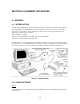
SECTION 6 ALIGNMENT PROCEDURE 6.1 GENERAL 6.1.1 INTRODUCTION The following alignment procedure should be performed if repairs are made that could affect the factory alignment or if adjustments may have changed for some other reason. To verify radio operation, the performance tests in Sections 6.5 and 6.6 can be run. To perform transceiver alignment, the following are required: • PC-compatible computer • Remote Programming Interface (RPI), Part No. 023-5300-000. • PCTune software, Part No. 023-9998-499.
• Windows® 95/98/NT/2000 (3.1 cannot be used) • Pentium® processor or equivalent • 16 MB of RAM • A hard disk drive with at least 3 MB of free space • A CD-ROM drive • An available serial port Software Installation Proceed as follows to install this software: 1. Close all applications that are currently running (other than Windows). 2. Insert the CD-ROM containing the PCTune software into the drive. 3. From the Windows taskbar, choose RUN and open SETUP.EXE on the drive being used.
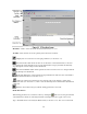
Menu Bar - Used to select the menus described in Sections 6.3.1-6.3.5. Tool Bar - These buttons are used to quickly select functions as follows: - Displays the screen used to set serial port parameters (see Section 6.3.3). - Selects the Partial Tune mode the same as the Transfer > Tune Partial menu (see Section 6.3.3) This mode allows manual selection of the desired Tune Category and then automatically steps through the various settings for that adjustment.
be selected for communication with the radio to occur. Band - The radio frequency band of the radio displayed after information is read from radio. Do not select the band using Tools > Set Band (Section 6.3.4) because this may make the radio nonfunctional. Software DSP - The first number is the version number of the radio firmware (Flash/operating code), and the second number is the version number of the DSP software. ESN - The Electronic Serial Number electronically stored in the radio.
(9600/ 19200) used for communication with the radio. Select the computer port to which the test cable is connected (see Section 6.4.1), and 19200 baud is normally selected. These parameters default to the last selected condition the next time the program is started. Read Tune Parameters - Selecting this function or clicking the button reads the tune parameters currently programmed in the transceiver and displays them in the various screens.
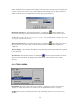
CAUTION: Do not select this function because it can make the radio non-functional. Reset Passwords - Erases all password information contained in the radio. This function can be used, for example, to allow reprogramming of passwords if they are lost. NOTE: Radio personality information is not erased by this function. Erase EEPROM CAUTION: This function erases important radio programming information as described below. Complete -Erases all EEPROM information, including factory programmed parameters.
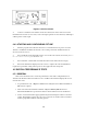
Figure 6-3 RPI Front Panel 4. Connect a wattmeter and a suitable load to the antenna jack of the transceiver for the transmitter tests. For the receiver tests, connect the signal generator to the antenna jack through a 6 dB or greater isolation pad. 6.4.2 STARTING AND CONFIGURING PCTUNE 1. Start the program as described in Section 6.1.2 and turn transceiver power on. Select Transfer > COM Port and make sure that the correct serial port and the 19200 baud rate are selected (see Section 6.3.3). 2.
NAC - 293 (hex) TGID (Talk Group ID) -1 Frequency - Any frequency in radio operating band 6.5.2 RECEIVE TEST SETUP 1. Connect the test setup and start and configure the PCTune software as described in Section 6.4. Select the Tools > Tx/Rx Tests menu to display the Tx/Rx Tests screen. Then in the Test Type drop-down list select Receive to display the following screen. 2. Connect the Digital Communication Monitor to the antenna jack using a 6 dB or greater isolation pad.
2. Select the Low Deviation test and set the analyzer as required to measure transmitter deviation. This test generates continuous repetitions of bits 10100000. Deviation should be 8481037 Hz. 3. Click the “PTT” button to transmit the tone. When finished, click that button again to turn the transmitter off. 4. Select the “High Deviation” test which transmits a standard transmitter test pattern. Deviation should be 2544-3111 Hz. 5.
3. Set the signal generator output level for 1000 µV (–47 dBm) at the antenna jack. 4. Decrease the signal generator output to obtain 12 dB SINAD. The signal generator output should be 0.35 µV (–116 dBm) or less for 25 kHz channels, or 0.50 µV (–113 dBm) or less for 12.5 kHz channels. Audio Power Output and Distortion 5. Connect a distortion meter across the speaker load. Return the generator output to 1000 µV. Distortion should be 3% or less. Squelch Sensitivity 6.
5. Select a channel programmed with Call Guard (CTCSS/DCS) signaling. Maximum total Call Guard and voice modulation should be approximately as follows: 12.5 kHz Channels - 2.3 kHz 25 kHz Channels - 4.
SECTION 7 PARTS LIST 65
SECTION 7 PARTS LIST Ref No. Description Part No.
MP 004 Gasket, blank front panel (remote) 032-0792-068 MP 005 Front panel, blank (remote) 032-0792-005 MP 156 Gasket, top cover 018-1136-136 MP 157 Gasket, bottom cover 018-1136-134 MP 300 Foam tape, dbl side 574-3002-013 MP 505 Grounding clip (rx/ex assy) 017-9700-003 MP 601 Shield, low-pass filter wrap around 017-9700-010 C 029 470 pF ±10% 25V cer smd 510-3681-471 CR 001 10V zener SOT-23 523-2016-100 CR 002 Switching diode SOT-23 523-1504-002 J 201 Connector, 20-pin 515-7111-230 J
R 018 10k ohm ±5% 1/8W smd 569-0115-103 R 019 Zero ohm jumper 569-0115-001 R 020 10k ohm ±5% 1/8W smd 569-0115-103 R 021 10k ohm ±5% 1/8W smd 569-0115-103 R 022 10k ohm ±5% 1/8W smd 569-0105-103 R 023 12k ohm ±5% 1/8W smd 569-0115-123 R 024 12k ohm ±5% 1/8W smd 569-0155-123 R 025 20k ohm ±5% 1/8W smd 569-0155-203 R 026 13k ohm ±5% 1/8W smd 569-0155-133 R 027 10k ohm ±5% 1/8W smd 569-0115-103 R 028 100k ohm ±5% 1/8W smd 569-0115-104 R 029 100k ohm ±5% 1/8W smd 569-0115-104
smd C 016 39 pF ±5% NPO 50V cer smd 510-3674-390 C 017 .
C 034 6.8 µF 35V SMD tant 510-2635-689 C 035 .001 µF ±5% chip 510-3602-102 C 067 330 pF NPO ±5% chp 510-3601-331 C 036 330 pF NPO ±5% chp 510-3601-331 C 069 330 pF NPO ±5% chp 510-3601-331 C 037 .018 µF X7R ±10% chp 510-3605-183 C 070 100 pF NPO ±5% chp 510-3601-101 C 038 6.8 µF 35V SMD tant 510-2635-689 C 071 330 pF NPO ±5% chp 510-3601-331 C 039 330 pF NPO ±5% chp 510-3601-331 C 072 .
C 560 1 µf 16V chip cap 510-3606-105 L 010 330 nH 0805 SMD 10% inductor 542-9003-338 L 011 2T .230” ID air die SMD inductor 016-0020-082 L 012 2T .230” ID air die SMD inductor 016-0020-082 L 013 2T .230” ID air die SMD inductor 016-0020-082 L 016 9700 DC line filter, fieldinstalled 542-5010-003 L 018 330 nH 0805 SMD 10% inductor 542-9003-338 L 019 220 nH 0805 SMD 10% inductor 542-9003-228 L 020 39 nH 0805 SMD 10% inductor 542-9003-397 L 021 3T .
R 007 10k ohm ±5% chip 569-0105-103 R 049 100 ohm ±5% chip 569-0105-101 R 008 4.3k ohm ±5% chip 569-0105-432 R 050 100 ohm ±5% chip 569-0105-101 R 009 20k ohm ±5% chip 569-0105-203 R 051 1.
LOGIC BOARD ASSEMBLY Part No. 023-5500-600 A 001 C 001 SEM encryption module 023-5000-980 C 184 .01 µF ±10% 10V cer smd 510-3681-103 C 185 .01 µF ±10% 10V cer smd 510-3681-103 C 186 .01 µF ±10% 10V cer smd 510-3681-103 C 190 .01 µF ±10% 10V cer smd 510-3681-103 C 191 .01 µF ±10% 10V cer smd 510-3681-103 C 192 .01 µF ±10% 10V cer smd 510-3681-103 C 196 .1 µF ±10% X7R 25V cer smd 510-3675-104 C 197 .1 µF ±10% X7R 25V cer smd 510-3675-104 C 198 .
C 217 .01 µF ±10% 10V cer smd 510-3681-103 C 246 1 µF ±20% Z5U 25V cer smd C 218 .01 µF ±10% 10V cer smd 510-3681-103 C 219 .01 µF ±10% 10V cer smd 510-3681-103 C 220 .01 µF ±10% 10V cer smd 510-3681-103 C 221 .01 µF ±10% 10V cer smd 510-3681-103 C 222 .01 µF ±10% 10V cer smd 510-3681-103 C 223 .01 µF ±10% 10V cer smd 510-3681-103 C 224 .01 µF ±10% 10V cer smd 510-3681-103 C 225 .01 µF ±10% 10V cer smd 510-3681-103 C 226 10 µF 10V cer smd 510-3755-106 C 227 .
smd C 272 470 pF ±5% NPO 25V cer smd 510-3674-471 470 pF ±5% NPO 25V cer smd 510-3674-471 470 pF ±5% NPO 25V cer smd 510-3674-471 470 pF ±5% NPO 25V cer smd 510-3674-471 470 pF ±5% NPO 25V cer smd 510-3674-471 470 pF ±5% NPO 25V cer smd 510-3674-471 470 pF ±5% NPO 25V cer smd 510-3674-471 470 pF ±5% NPO 25V cer smd 510-3674-471 470 pF ±5% NPO 25V cer smd 510-3674-471 470 pF ±5% NPO 25V cer smd 510-3674-471 470 pF ±5% NPO 25V cer smd 510-3674-471 470 pF ±5% NPO 25V cer smd 510-3674-47
C 328 .01 µF ±10% 10V cer smd 510-3681-103 CR 003 Silicon switching diode 523-1004-021 C 329 .01 µF ±10% 10V cer smd 510-3681-103 CR 004 Zener diode, 5.6V 523-2016-569 C330 .01 µF ±10% 10V cer smd 510-3681-103 CR 005 Zener diode, 18V 523-2601-180 C331 .01 µF ±10% 10V cer smd 510-3681-103 CR 006 Zener diode, 5.1V 523-2601-519 C332 .1 µF ±10% X7R 25V cer smd 510-3675-104 CR 010 Zener diode, 3.6V 523-2016-369 CR 011 Zener diode, 3.6V 523-2016-369 C333 .
L 055 Bead, ferrite smd 542-9230-005 R 002 51k ohm ±5% 1/16W smd 569-0165-513 L 056 Bead, ferrite smd 542-9230-005 R 003 51k ohm ±5% 1/16W smd 569-0165-513 L 057 Inductor, ferrite smd 542-9230-021 R 004 51k ohm ±5% 1/16W smd 569-0165-513 L 058 Inductor, ferrite smd 542-9230-021 R 006 4.7k ohm ±5% 1/16W smd 569-0165-472 L 059 Inductor, ferrite smd 542-9230-021 R 007 4.7k ohm ±5% 1/16W smd 569-0165-472 L 060 Inductor, ferrite smd 542-9230-021 R 008 4.
R 102 4.
R 293 6.8k ohm ±5% 1/16W smd 569-0155-682 R334 47k ohm ±5% 1/16W smd 569-0155-473 R 294 100k ohm ±5% 1/16W smd 569-0155-104 R336 100 ohm ±5% 1/16W smd 569-0155-101 R 295 150 ohm ±5% 1/16W smd 569-0155-151 R338 10k ohm ±5% 1/16W smd 569-0155-103 R 296 6.
R 399 100k ohm ±5% 1/16W smd 569-0165-104 R 709 1k ohm ±5% 1/16W smd 569-0165-102 R 400 634k ohm ±1% 0.1W smd 569-0151-578 R 710 1k ohm ±5% 1/16W smd 569-0165-102 R 401 100k ohm ±1% 0.1W smd 569-0151-501 R 711 1k ohm ±5% 1/16W smd 569-0165-102 R 402 100k ohm ±5% 1/16W smd 569-0165-104 R 712 1k ohm ±5% 1/16W smd 569-0165-102 R 403 255k ohm ±1% 0.1W smd 569-0151-551 R 713 10k ohm ±5% 1/16W smd 569-0165-103 R 404 100k ohm ±1% 0.
R 748 10 ohm ±5% 1/16W smd 569-0165-100 R 749 10 ohm ±5% 1/16W smd 569-0165-100 R 752 10k ohm ±5% 1/16W smd 569-0165-103 R 753 10k ohm ±5% 1/16W smd 569-0165-103 S 001 T 001 Switch, momentary norm open Isolation transformer 10BASE-T 583-9512-002 592-9017-003 U 001 DSP TMS3205510AGGWA1 544-5003-133 U 002 CODEC, dual TLV320AIC211 544-3016-057 U 003 Schmitt trig, inv TC7S14FTE85L 544-3123-014 U 004 Op Amp OPA340NA 544-2020-023 U 011 Regulator, 5V 400mA 544-2603-055 REG113EA-5 U
Y 003 TCXO, 12.288 MHz smd 518-7012-200 Y 004 Oscillator, 20.000 MHz smd 561-9004-200 FRONT PANEL ASSEMBLY Part No.
S 001 DIP switch, 10-position 583-5100-210 S 154 On-off/Vol push on w/50k pot std 562-0018-075 On-off/Vol rot on-off , motorcycle 562-0018-077 Switch rotary and push 583-2042-001 S 155 U 710 LCD driver, PCF8576TD 544-2027-010 U 711 LCD driver, PCF8576TD 544-2027-010 U 712 Regulator, 8V 0.5A 78M08 544-2003-081 C 020 .01µF ±10% X7R cer smd 510-3675-103 C 021 .1 µF ±10% X7R 50V cer smd 510-3675-104 C 022 .1 µF ±10% X7R 50V cer smd 510-3675-104 C 023 .
J 701 Connector, micro-miniature 515-7113-073 R 028 100k ohm ±5% 1/16W smd 569-0155-104 J 702 Connector, 9-pin ZIF flex 515-7111-321 R 029 100k ohm ±5% 1/16W smd 569-0155-104 J 704 Connector, 5-pin (PA bd cable) 515-7111-254 R 030 10k ohm ±5% 1/16W smd 569-0155-103 R 031 300ohm ±5% 1/16W smd 569-0155-301 R 032 47k ohm ±5% 1/16W smd 569-0155-473 R 033 47k ohm ±5% 1/16W smd 569-0155-473 R 035 47k ohm ±5% 1/16W smd 569-0155-473 R 036 620 ohm ±5% 1/8W smd 569-0105-621 R 037 620
R 068 10k ohm ±5% 1/16W smd 569-0155-103 R 110 10k ohm ±5% 1/16W smd 569-0155-103 R 069 10k ohm ±5% 1/16W smd 569-0155-103 R 111 47k ohm ±5% 1/16W smd 569-0155-473 R 070 10k ohm ±5% 1/16W smd 569-0155-103 R 112 100k ohm ±5% 1/16W smd 569-0155-104 R 071 47k ohm ±5% 1/16W smd 569-0155-473 R 113 100k ohm ±5% 1/16W smd 569-0155-104 R 072 10k ohm ±5% 1/16W smd 569-0155-103 R 114 100k ohm ±5% 1/16W smd 569-0155-104 R 073 10k ohm ±5% 1/16W smd 569-0155-103 R 115 1k ohm ±5% 1/16W s
003 MP 001 Knob, remote control unit 032-0792-015 MP 002 Mounting bracket, rem ctrl unit 017-2226-050 MP 003 Gasket 032-0792-066 MP 005 Housing, remote control unit 032-0792-130 EP 003 Ring terminal, 3/8 10-12 AWG 586-0001-019 F 101 Fuse, 15 amp 32V 534-0003-038 HW 000 Key extraction tool 017-2226-000 HW 002 Screw, 4-40 x 3/8 pan head (1) 575-0604-012 HW 003 Screw, 4-24 x 1/4 phil (3) 575-3604-008 Screw, 4-20 x 5/8 phil (3) 575-5604-020 MP 006 Rear cover, remote control unit 032-0792
S 001 Front Mounting Bracket Assembly Part No. 023-9750-012 Leaf switch SPST 583-1004-031 15 Watt, 4.0-Ohm Speaker (Black) HW 001 Self-drilling screw 1/4 (4) 575-9077-565 HW 002 Self-drilling screw #10 (4) 575-9077-545 Part No.
MP004 Tri knob 10-32 547-0016-004 NP001 Overlay, speaker front 559-0072-010 S 001 583-0006-061 Switch, SPST toggle W 001 Speaker wire, motorcycle 023-0151-011 88
Ref No. Description smd Part No. HANDHELD CONTROL UNIT Part No. 250-5300-101 C 022 0.1 µF ±10% X7R 25V cer 510-3675-104 smd C 023 0.1 µF ±10% X7R 25V cer 510-3675-104 smd C 025 180 pF ±5% NPO 25V cer 510-3674-181 smd A 001 Main board assembly 023-5300-705 A 002 Keypad board assembly 023-5300-707 C 029 1.0 µF 10V tantalum smd 510-2624-109 A 130 Junction box assembly 023-5300-130 C 030 10 µF 25V tantalum smd 510-2627-100 C 031 4.7 µF 20V tantalum smd 510-2626-479 C 032 0.
C 146 0.1 µF ±10% X7R 25V cer 510-3675-104 smd CR 004- 5.6V zener backlighting 523-2016-569 CR 11 CR 012 Pin switching diode 523-1504-001 CR 013 5.6V zener 523-2016-569 CR 020 5.6V zener 523-2016-569 CR 021 5.6V zener 523-2016-569 CR 023 5.6V zener 523-2016-569 CR 024 Dual color LED, red/grn 549-4001-215 CR 025- 5.
R 007 47k ohm ±5% 1/16W smd 569-0155-473 R 065 10k ohm ±5% 1/16W smd 569-0155-103 R 008 47k ohm ±5% 1/16W smd 569-0155-473 R 066 3.3k ohm ±5% 1/16W smd 569-0155-332 R 009 47k ohm ±5% 1/16W smd 569-0155-473 R 067 2.2k ohm ±5% 1/16W smd 569-0155-222 R 010 47k ohm ±5% 1/16W smd 569-0155-473 R 068 10k ohm ±5% 1/16W smd 569-0155-103 R 011 2.2k ohm ±5% 1/16W smd 569-0155-222 R 069 10k ohm ±5% 1/16W smd 569-0155-103 R 012 2.
R 110 10k ohm ±5% 1/16W smd 569-0155-103 R 153 1k ohm ±5% 1/8W smd 569-0115-102 R 111 47k ohm ±5% 1/16W smd 569-0155-473 R 154 1k ohm ±5% 1/8W smd 569-0115-102 R 112 100k ohm ±5% 1/16W smd 569-0155-104 R 155 1k ohm ±5% 1/8W smd 569-0115-102 R 113 100k ohm ±5% 1/16W smd 569-0155-104 R 156 1k ohm ±5% 1/8W smd 569-0115-102 R 114 100k ohm ±5% 1/16W smd 569-0155-104 R 115 1k ohm ±5% 1/16W smd 569-0155-102 S 001 10 Pos DIP switch 583-5100-210 R 116 47k ohm ±5% 1/16W smd 569-0155-473
HHC Junction Box Assembly Part No. 023-5300-130 510-2626-229 C 026 0.1 µF ±10% X7R 25V cer 510-3675-104 smd C 027 0.1 µF ±10% X7R 25V cer 510-3675-104 smd C 001 2.2 uF 20V tantalum smd C 002 0.1 µF ±10% X7R 25V cer 510-3675-104 smd C 028 1µF X7R ±10% 16V cer smd C 003 0.1 µF ±10% X7R 25V cer 510-3675-104 smd C 029 0.1 µF ±10% X7R 25V cer 510-3675-104 smd C 004 2.2 uF 20V tantalum smd C 030 C 005 0.1 µF ±10% X7R 25V cer 510-3675-104 smd 0.1 µF ±10% X7R 25V cer 510-3675-104 smd C 006 0.
R 004 39k ohm ±5% 1/16W smd 569-0155-393 R 040 20k ohm ±5% 1/16W smd 569-0155-203 R 005 62k ohm ±5% 1/16W smd 569-0155-623 R 041 100k ohm ±5% 1/16W smd 569-0155-104 R 006 62k ohm ±5% 1/16W smd 569-0155-623 R 042 20k ohm ±5% 1/16W smd 569-0155-203 R 007 10k ohm ±5% 1/16W smd 569-0155-103 R 043 20k ohm ±5% 1/16W smd 569-0155-203 R 008 1k ohm ±5% 1/16W smd 569-0155-102 R 044 20k ohm ±5% 1/16W smd 569-0155-203 R 009 2.
HW001 Ring terminal, 1/4 12-16 AWG 586-0001-150 HW002 Solder splice terminator .100-.175 586-0007-085 W 001 Wire, zip cord 14 AWG 597-2006-004 W 002 Wire, 14 AWG black stranded 597-7021-400 W 003 Wire, 14 AWG red stranded 597-7021-402 REMOTE PROG. INTERFACE (RPI) Part No.
U 004 RS-232 rx/tx, dual MAX232 544-2023-019 U 005 RS-485 bus xcvr SN65176 544-2023-027 U 006 Ref No. Schmitt trigger 74HC14 544-3766-014 Description Part No.
C30,C293 CAP, PPS FILM, 0.22 UF, ±10%, 25V, LOW ESR, 3216 1C478-224 C31,C139 CAP, CER, 200 PF, ±5%, NPO, 0603 1C113-201 C32 CAP, TANT, 4.7 UF, ±20%, 16V, B CASE 1C166-475 C35,C125,C132,C133,C168,C171,C174,C175,C202,C203,C286, C289,C290,C302 CAP, TANT, 4.7 UF, ±20%, 16V, A CASE 1C573-A475 C38,C115 CAP, CER, 33 PF, ±5%, NPO, 0603 1C113-330 C39 CAP, CER, 8.2 PF, ±0.25 PF, 0603 1C450-8R2 C40 CAP, CER, 1.0 PF, ±0.
C306 CAP, FILM CHIP, 1200 PF, ±5%, 16V, 0805 73697 C308 CAP, FILM CHIP, 4700 PF, ±5%, 16V, 0805 73699 C309 CAP, FILM CHIP, 3300 PF, ±5%, 16V, 0805 73698 D4,D10 TRANS, MOSFET, P-CH, SOT23 1T158SI2323 D9 DIODE, SILICON, TUNING, SOT23, MV2105 72672 D12,D13 DIODE, PIN, HIGH AVG POWER SMQ, MELF 72663 EC1 SHIELD,COVER, IF LARGE 3M797-2 EC2 SHIELD, COVER, IF SMALL 3M809-2 EC5 SHIELD, COVER, PLL 3M813-2 EC7 SHIELD, POWER AMPLIFIER 3M800 EC9 CLIP, GROUND, 3638001000 72673 EC10 CLIP,
L35 INDUCTOR, 39 NH, ±5%, SMT, 0603 1L177-390 L40 INDUCTOR, 100 NH, ±5%, SMT, 0603 1L177-101 L44 INDUCTOR, 82 NH, ±5%, SMT, 0603 1L177-820 L46,L47,L48 INDTR, CHIP, 470 NH, 5%, 0603LS 1L835-471 L50,L51,L53,L54 INDTR, 150 NH, ±2%, SMT, 1008 (REFERENCE 78127) 1L498-151 L77,L78 INDTR, 72 NH, ±2%, SMT, 0603 1L177-720G L81 INDUCTOR, 330 NH, ±5%, SMT, 0603 1L177-331 MX1 MIXER, 100-500 MHZ, 7 DB CL, 5 DBM LO 72668 P4,P5,P6,P7,P8 SPRING CONTACT,ELECTRICAL 3C799 Q1,Q2 TRANSISTOR, SMT, NPN, S
R38 RES, 6.2K, ±5%, SMT, 0603 1R105-622 R39 RES, 36K, ±5%, SMT, 0603 1R105-363 R41 RES, 15K, ±5%, SMT, 0603 1R105-153 R44 RES, 3K OHM, ±5%, SMT, 0603 1R105-302 R46,R54 RES, 220 OHM, ±5%, SMT, 0603 1R105-221 R47,R49,R71,R119 RES, 100 OHM, ±5%, SMT, 0603 1R105-101 R50 RES, 24 OHM, ±5%, SMT, 0603 1R105-240 R51 RES, 3.9K OHM, ±5%, SMT, 0603 1R105-392 R53 RES, 4K OHM, ±5%, SMT, 0603 1R105-473 R55,R61 RES, 100K OHM, ±5%, SMT, 0603 1R105-104 R56 RES, 1.