
Data Sheet

Module:EWN-8258FAT1CC
Waiting for your suggestion at anytime.
-
9 -
E-mail:sales@eardatek.com
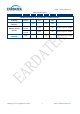
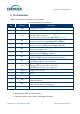
8 Pin Definition
Table 6 the hardware Pin definition of the module
Table 6 EWN-8258FAT1CC Pin definition
PIN Definition Description
1 VBAT Supply power 1.8V-3.3V;
2 GND Ground
3 PC3
PWM1 output / UART_RX / I2C serial clock /
(optional) 32kHz crystal input /
PGA right channel negative input / GPIO PC[3]
4 PB4
SDM positive output 0 /PWM4 output
/ Low power comparator input / SAR ADC input / GPIO PB[4]
5 PB5
SDM negative output 0 / PWM5 output /
Low power comparator input / SAR ADC input / GPIO PB[5]
6 PC4
PWM2 output / UART_CTS / PWM0 inverting output /
SAR ADC input / GPIO PC[4]
7 PC1
I2C serial clock / PWM1 inverting output / PWM0 output /
PGA left channel negative input / GPIO PC[1]
8 PB7
SDM negative output 1 / SPI data output / UART_RX /
Low power comparator input / SAR ADC input / GPIO PB[7]
9
PC0
I2C serial data / PWM4 inverting output / UART_RTS /
PGA left channel positive input / GPIO PC[0]
10
PC2
PWM0 output / UART 7816 TRX (UART_TX) /
I2C serial data / (optional) 32kHz crystal output /
PGA right channel positive input / GPIO PC[2]
11
RST Power on reset, active low;
12
GND Ground
13
SWS Single wire slave;
14
PA0
DMIC data input / PWM0 inverting output /
UART_RX/ GPIO PA[0]
15
PD7
SPI clock (I2C_SCK) / I2S bit clock /
UART 7816 TRX (UART_TX) / GPIO PD[7]
16
GND Ground
Notes:
1. Download Interface use SWS test point.
2. Only SWS interface can be used for debugging firmware.