
Cut Sheet
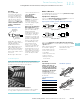

V8-T12-34 Volume 8—Sensing Solutions CA08100010E—November 2012 www.eaton.com
12
12
12
12
12
12
12
12
12
12
12
12
12
12
12
12
12
12
12
12
12
12
12
12
12
12
12
12
12
12
12.1
Sensor Learning Course
Learning Module 23: Limit Switches, Proximity Sensors and Photoelectric Sensors
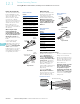
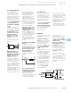
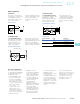
AC Power Cycle
As long as a triac is used
within its rated maximum
current and voltage
specification, life expectancy
is virtually infinite. Triac
devices used with sensors
are generally rated at 2A
loads or less, and can be
directly interfaced with PLCs
and other electronic devices.
Triacs do have some
limitations in that an inductive
load directly connected can
false trigger it. A snubber
circuit can be used to
minimize the problem.
Shorting the load will destroy
a triac, so the device should
be short circuit protected to
avoid this.
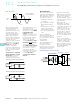
A transistor is a solid-state
device designed to control
DC current. They are most
commonly used in low
voltage DC powered sensors
as the output switch. There
are two types used,
depending on the switching
function. One is called NPN
(current sink) open
collector. The output
transistor is connected to the
negative DC. Current flows
from the positive terminal
through the load, to the
sensor, to the negative
terminal. The sensor “sinks”
the current from
the load.
The second type used is
called PNP (Current Source).
The sensor is connected to
the positive DC. Current
flows from the positive
terminal through the sensor,
to the load, to the negative
terminal. The sensor
“sources” the current to
the load.
Transistor Output Circuit (Sinking)
Transistor Output Circuit (Sourcing)
0
Contact
Vac
60 Hz
1 Cycle
Time
1 Cycle = 16.66 ms
1/2 Cycle = 8.33 ms
Circuit
B
C
E
36V
+V
Output
Common
36V
+V
Output
Common
Circuit
C
B
E
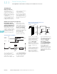
Bilateral FET Device
Photosensors have another
output type called a bilateral
FET output. This output has
many advantages over the
other types of outputs:
●
Switching of either AC or
DC voltages
●
Low “OFF-state” leakage
●
Extremely fast response
time
●
Interface direct to TTL and
CMOS circuits (for PLCs
and industrial computers)
●
Does not self-generate line
noise
FET is for Field Effect
Transistor, and may become
the most popular output in
the future because of its near
ideal operating
characteristics.
The voltage applied to the
gate (G) controls the
conduction resistance
between the source (S) and
drain (D). Because an FET is a
resistive device, it doesn’t
develop the fixed voltage
drop across its terminals like
other solid-state switches. It
also does not require any
residual or leakage current to
keep the electronics powered
in the OFF-state.
FET switches are
independent of voltage or
current phase and can be
configured in circuits that will
control either AC or DC
voltages. For circuits using
PLCs, computers or other
sensitive devices, FETs are
good because they do not
generate any switch induced
line noise like relay and triac
switches.
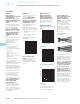
Like the other solid-state
outputs, they cannot tolerate
line spikes or large inrush
currents. In the illustration
above, a transorb is used to
protect the FET from voltage
spikes and dissipate the
energy as heat.
Bilateral FET Device (AC/DC Switch)
To
Photoelectric
Control Circuit
Opto-Coupler Photo
Voltaic Diode Stack
Transorb
Bilateral FET
To
AC/DC
Load
Circuit
D
G
S
D
G
S
+