® LONWORKS FTT-10A Free Topology Transceiver User’s Guide Version 3 @ E C H E L O N® Corporation 078-0156-01C
Echelon, LON, LONW ORKS , LonBuilder, NodeBuilder, LonManager, LonTalk, LONMARK , Neuron, 3120, 3150, the LonUsers logo, the LONMARK logo, and the Echelon logo are trademarks of Echelon Corporation registered in the United States and other countries. LonLink, LonSupport, and LonMaker are trademarks of Echelon Corporation. Other brand and product names are trademarks or registered trademarks of their respective holders.
Contents 1 Introduction Applications Audience Content Related Documentation 2 Electrical Interface Transceiver Pinout Network Connection Clock Input Neuron® Chip Communications Port (CP) Lines PC Board Layout Guidelines Physical Layer Repeater 3 Mechanical Considerations Mechanical Footprint 4 Network Cabling and Connection Network Overview System Performance and Cable Selection System Specifications Transmission Specifications Cable Termination 5 Design Issues EMI Design Issues Designing Systems f
Appendix A Guidelines for FTT-10 Users Mechanical Differences Pinout and External Circuit Differences Replacement in Existing PC Board Designs External Component Removal from an Existing Board Layout EMI Comparison Scans for the FTT-10 and FTT-10A Transceivers Comparison of FTT-10 and FTT-10A Radiated EMI SLTA-10 Adapter EN 55022-B Test Scan Appendix B FTT-10A Transceiver-Based Node Checklist FTT-10A Transceiver and Neuron Chip Connections FTT-10A PCB Layout FTT-10A Transceiver Programming FTT-10A Tran
1 Introduction The FTT-10A Free Topology Twisted Pair Transceiver provides a simple, cost-effective method of adding a LONWORKS transceiver to any Neuron® Chip-based control system. A replacement for the popular FTT-10 transceiver, the FTT-10A transceiver supports polarity insensitive, free topology wiring, freeing the system installer from the need to wire using a bus topology (differences between the FTT-10A and FTT-10 transceivers are described in Appendix A).
protects the transceiver should conformal coating or other forms of environmental sealing be required on the printed circuit assembly. The FTT-10A transceiver is compatible with Echelon's LPT-10 Link Power Transceiver, and these transceivers can communicate with each other on a single twisted pair cable. This capability provides an inexpensive means of interfacing to nodes whose current or voltage requirements would otherwise exceed the capacity of the link power segment.
Applications A conventional control system using bus topology wiring (such as RS-485) consists of a network of sensors and control outputs that are interconnected using a shielded twisted wire pair. In accordance with RS-485 guidelines, all of the devices must be wired in a bus topology to limit electrical reflections and ensure reliable communications. There is a high cost associated with installing and maintaining the cable plant that links together the many elements of an RS-485based control system.
best suits the installation, reducing the need for advanced planning and allowing last minute changes at the installation site. Second, if installers have been trained to use one style of wiring for all installations, free topology technology can be introduced without requiring retraining. Third, retrofit installations with existing wiring plants can be accommodated with minimal, if any, rewiring.
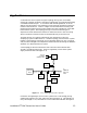
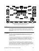
LP Node FT Node FT Node FT Node FT Node Term. FT Node FT Node FT Node LPI-10 FT Node Term. LP Node Power Supply LPT-10 FTT-10A FTT-10A FTT-10A FTT-10A FTT-10A FT Node 6-way repeater FT Node LP Node LPI-10 FT Node Term. FT Node FT Node FT Node FT Node LP Node FT Node FT Node Term. FTT-10A 2-way repeater Power Supply LP Node FT Node LP Node LPT-10 LPI-10 FT Node FT Node Term. Figure 1.
Related Documentation The following Echelon documents are suggested reading: LonBuilder User's Guide (078-0001-01) NodeBuilder User's Guide (078-0141-01) Neuron C Programmer's Guide (078-0002-01) LonBuilder Startup and Hardware Guide (078-0003-01) L ON M ARK ™ Layers 1-6 Interoperability Guidelines (078-0014-01) L ON M ARK ™ Application Layer Interoperability Guidelines (078-0120-01) Neuron Chip Data Book (published by Motorola and Toshiba) L ON W ORKS FTT-10A Free Topology Transceiver data sheet (003-0111-
2 Electrical Interface The FTT-10A Free Topology Transceiver provides a polarity insensitive connection to the twisted pair network, an interface to the Neuron Chip communications port, and a physical layer repeater function for expanding the size of a network.
Transceiver Pinout The pinout of the FTT-10A transceiver is shown in table 2.1. Table 2.2 lists the electrical specifications of the FTT-10A transceiver. All specifications apply over the full operating temperature and supply voltage ranges unless otherwise noted. Table 2.
Figure 2.1 is not a complete schematic, since the clock, reset and power supply bypass circuits will vary depending on the Neuron Chip type and application. For complete Neuron Chip application schematics and information, refer to the Neuron Chip Databook2,3. See chapter 3 for mechanical specifications and printed circuit board (PCB) footprint information.
onto the network wiring. The physical placement of Z1 and Z2 should be near the entry points of the network wiring with a low impedance path to chassis ground (or alternately to star ground near star ground center). The external components for figure 2.2 are shown in table 2.4. See Text C3 Neuron Chip (Partial) D5 D4 D6 NET2 FTT-10A CP0 RXD NET_A CP1 TXD NET_B CLK2 CLK VCC CP2 CP3 CP4 D3 NET1 +5V T1 T2 GND Z1 Z2 C2 C4 +5V D1 D2 C1 Figure 2.
contact-discharge method for electrostatic discharge (ESD) in accordance with IEC 1000-4-2. Note that it is the operation of the Neuron Chip, and not of the FTT-10A transceiver, which is affected at higher air-discharge levels when using the modified circuit. It is recommended that the simplified circuit be used only after determining that contact-discharge ESD protection is acceptable for the application.
Neuron Chip Communications Port (CP) Lines The FTT-10A transceiver transmits and receives LonTalk network packets via the Neuron Chip’s direct, single-ended mode interface using pins CP0 and CP1. Neuron Chip data input pin CP0 is connected to the RXD pin of the FTT-10A transceiver. Neuron Chip data output pin CP1 is connected to the TXD pin of the FTT-10A transceiver. No buffering or other connections should be made to CP1.
1. "Star" Ground Configuration: The distribution of functional circuit blocks on the PCB should be in the form of a star, with the power connector, network connector and any "chassis ground" connection all located as close as practical to the center of the star. This star ground distribution is illustrated in figure 2.4. The goal of star ground distribution is to conduct transients out of the node with minimal disruption to other function blocks.
Component Side D2 D1 VCC Net C1 VCC T2 Solder Side (X-ray view) GND T1 VCC CLK T2 GND CLK T1 TXD TXD RXD RXD Keep-out area NET_B NET_A NET_B NET_A Star Ground Center C2 D3 D4 C3 C4 Spark Gap (2X) 2.30mm 0.090" 1.78mm 0.070" 1.00mm 0.040" Solder Mask Ground Plane PCB 0.51mm 0.019" Dia. Via Spark Gap Detail Cross-section Figure 2.
Application I/O Block Neuron Chip Block Clock Ground Guard Power Supply Block Star Ground Center Figure 2.
5. Ground Planes: As ground is routed from the center of the star out to the function blocks on the board, planes or very wide traces should be used to lower the inductance (and therefore the impedance) of the ground distribution system. 6. +5V Power Distribution & Decoupling: In general, Vcc should be distributed through low inductance traces and planes in the same manner as ground. At least two 0.
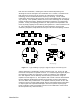
Network Segment 1 Network Segment 2 Network Segment 1 FTT-10A Transceiver FTT-10A Transceiver FTT-10A Transceiver N-Way Repeater Two-Way Repeater FTT-10A Transceiver FTT-10A Transceiver Network Segment 2 FTT-10A Transceiver Network Segment 3 Network Segment N Figure 2.5 Two-Way and N-Way Repeaters A repeater consists of two or more transceivers, a 5MHz clock source, and miscellaneous components. Figures 2.6 and 2.7 show schematics for two-way and N-way repeaters, respectively.
UA See Text FTT-10A TXD C3A NET_A RXD NET_B CLK VCC NET1 C4A NET2 +5V D1A C1A PCB Spark Gaps R1A T1 C5A D2A T2 R2A GND UB See Text FTT-10A TXD NET_A RXD NET_B CLK VCC C3B NET1 C4B NET2 +5V D1B T1 5MHz Clock Oscillator C1B PCB Spark Gaps R1B C5B D2B T2 GND R2B R1 1500Ω, 1% R2 576 Ω, 1% C5 0.1 µF, X7R or Y5V ceramic Other components per Table 2.3 Operating temperature range: 0 to +85°C Figure 2.
UA See Text FTT-10A TXD C3A NET_A RXD NET_B CLK VCC NET1 C4A NET2 +5V D1A T1 C1A PCB Spark Gaps R1A C5A D2A T2 R2A GND UB See Text FTT-10A TXD C3B NET_A RXD NET_B CLK VCC NET1 C4B NET2 +5V D1B C1B PCB Spark Gaps R1B T1 C5B D2B T2 R2B GND N-Input OR UN See Text FTT-10A TXD NET_A RXD NET_B CLK VCC C3N NET1 C4N NET2 +5V D1N C1N R1N T1 C5N D2N 5MHz Clock Oscillator PCB Spark Gaps T2 GND R2N R1 1500Ω, 1% R2 576 Ω, 1% C5 0.
3 Mechanical Considerations This chapter discusses the mechanical footprint and pin locations of the FTT-10A Free Topology Transceiver.
Mechanical Footprint The FTT-10A transceiver mechanical dimensions are shown in figures 3.1 through 3.4. The transceiver is mounted to the application board as a throughhole, soldered component. Decisions about component placement on the application electronics board must also consider electromagnetic interference (EMI) and electrostatic discharge (ESD) issues as discussed elsewhere in this document. 7.2mm (0.28") max. 3mm (0.12") min. Figure 3.
6 5 4 3 CLK TXD RXD NET_A 7 T1 11.94 ±0.5 10.16 8 GND 7.62 5.08 9 T2 2.54 1 ±0.5 1.78 ECHELON FTT-10A 50051 2 VCC NET_B 5.02 7.62 12.70 2.10 ±0.5 15.70 ±0.5 Pin locations are ±0.25mm from ideal 2.54mm grid Pin diameter is 0.60+0.10/-0.15 mm Figure 3.3 FTT-10A Transceiver Top “X-RAY” View – dimensions in mm 6 5 4 3 CLK TXD RXD NET_A 7 T1 0.47 ±0.02 0.40 8 GND 0.30 0.20 9 T2 0.10 1 0.07 ±0.02 ECHELON FTT-10A 50051 2 VCC NET_B 0.20 0.30 0.50 0.08 ±0.
4 Network Cabling and Connection This chapter provides information about cabling and network connections for the FTT-10A Free Topology Transceiver.
Network Overview The TP/FT-10 network is designed to support free topology wiring, and will accommodate bus, star, loop, or any combination of these topologies. FTT-10A transceivers can be located at any point along the network wiring. This capability simplifies system installation and makes it easy to add nodes should the network need to be expanded. Figures 4.1 through 4.5 present five different network topologies. Termination Figure 4.
Termination Figure 4.4 Loop Topology Termination Figure 4.5 Mixed Topology In the event that the limits on the number of transceivers or total wire distance are exceeded, then an FTT physical layer repeater can be added to interconnect two segments and double the overall system capability (see chapter 2). The FTT-10A transceiver can also be used with LONW ORKS Routers to interconnect a TP/FT10 channel with another TP/FT-10 channel, or with any other LONWORKS channel.
System Performance and Cable Selection TP/FT-10 network system and transmission specifications are outlined on the following pages. Both of these specifications must be met to ensure proper operation. The system designer may choose a variety of cables, depending on cost, availability, and performance. Performance may vary with cable type. The transmission specification depends on such factors as resistance, mutual capacitance, and the velocity of propagation.
Transmission Specifications Table 4.2 Doubly-Terminated Bus Topology Specifications Maximum bus length Belden 85102 2700 Belden 8471 2700 Level IV, 22AWG 1400 JY (St) Y 2x2x0.8 900 TIA Category 5 900 Units meters A doubly-terminated bus may have stubs of up to 3 meters from the bus to each node. Table 4.3 Free Topology Specifications Maximum node-to-node distance Maximum total wire length Belden 85102 500 500 Belden 8471 400 500 Level IV, 22AWG 400 500 JY (St) Y 2x2x0.
Cable Termination The FTT-10 network segment requires termination for proper data transmission performance. A total termination impedance of approximately 52.3Ω is required. Free Topology Segment In a free topology segment, only one termination is required and may be placed anywhere on the free topology segment. There are two choices for the termination: 1. RC network (figure 4.6), with R1 = 52.3Ω±1%, 1/8W 2. LPI-10 Link Power Interface, with jumper at "1 CPLR" setting.
5 Design Issues This chapter looks at design issues, and includes discussions of electromagnetic interference (EMI), electrostatic discharge (ESD), vibration, shock, and IEC 1000-4 testing for the FTT-10A Free Topology Transceiver.
EMI Design Issues The high-speed digital signals associated with microcontroller designs can generate unintentional electromagnetic interference (EMI). High-speed voltage transitions generate RF currents that can cause radiation from a product if a length of wire or piece of metal can serve as an antenna. Products that use an FTT-10A transceiver together with a Neuron Chip will generally need to demonstrate compliance with EMI limits enforced by various regulatory agencies.
"Floating" Node on FTT-10A Network FTT-10A Vcc Vcc Vgate Twisted Pair Network C decouple NET_A C load NET_B Node Logic Ground GND Leakage Capacitances to Earth Ground "CHASSIS" GND C leak,CHASSIS C leak,GND C leak,SIGNAL Figure 5.1 Parasitic Leakage Capacitances to Earth Ground From this discussion, it is apparent that minimizing Cleak,SIGNAL is very important. By using 0.1µF or 0.01µF decoupling capacitors at each digital IC power pin, Vcc and logic ground noise can be reduced.
and may require a four-layer PCB to maintain an RF-quiet Vcc and logic ground. Some FTT-10A nodes with fast digital circuitry, such as DSP engines and memory arrays, may require extra RF attenuation between the FTT-10A transceiver and the twisted pair network in order to meet FCC/CISPR level "A" or "B". This extra attenuation can be provided by a ferrite bead (muRata BLM11A601 or equal) in series with each network line adjacent to the network connector.
• ferrite beads in series with the network traces at the network connector, and ferrite chokes in series with the power input traces at the power connector, can be used to help meet EMC requirements for nodes that have noisy application circuitry or special circuit requirements. Early testing of prototype circuits at an outdoor EMI range should be used to determine the effectiveness of these EMC techniques in a particular application.
then out to the product's chassis or earth ground connection. If the node is floating with respect to earth ground, the ESD current will return capacitively to earth via the network wire, the power supply wires, and the PCB ground plane. Designers of FTT-10A transceiver-based nodes should follow the PCB layout guidelines presented in chapter 2. In addition, external clamping of useraccessible circuitry is required to shunt ESD currents from that circuitry to the center of the star ground on the PCB.
IEC Electromagnetic Compatibility (EMC) Testing Echelon has tested the FTT-10A transceiver operating in typical two-layer application boards to verify that the transceiver complies with the four applicable IEC 1000-4 test requirements. As long as a node's PCB is designed following the guidelines in chapter 2, the FTT-10A transceiver should pass the following IEC 1000-4 tests: Table 5.
For more information on levels and installation classes, see IEC 1000-4-5. The applicable surge test levels and coupling mode specified by IEC 1000-4-5 can be found in table A.1 of [16] as follows: 5-8 Issues • balanced circuits/lines; • coupling mode is line-to-ground, either polarity; • surge waveform is 1.2/50µs (8/20µs) combination wave for classes 1-4.
6 Programming Considerations This section explains the integration of the FTT-10A Free Topology Transceiver using the LonBuilder Developer’s Workbench and NodeBuilder Development Tool. It covers considerations relating to channel definition and custom node image generation.
Application Program Development and Export Application programs are initially developed, tested, and debugged using the LonBuilder Developer’s Workbench or the NodeBuilder™ Development tool. See the LonBuilder User’s Guide and NodeBuilder User’s Guide for detailed instructions on developing and testing applications. Actual unit and system testing on the TP/FT-10 channel requires one or more Echelon Model number 77040 FTM-10 Standard Modular Transceivers (SMX™).
Two or more FTT-10A transceivers can function as a physical layer repeater to extend the size of the network. The standard channel definition shown in table 6.2 accommodates the delay that occurs as a packet is forwarded by a single physical layer repeater. If additional repeaters will exist in the path of a packet, the Rcv Start Delay, and Missed Pream parameters for the channel definition must be modified according to the notes shown in table 6.2.
• Select a TP/FT-10 channel in the protocol analyzer Network Mgmt.Target HW definition; • Mount an FTM-10 Modular Transceiver on a LonBuilder SMX Adapter; • Mount the LonBuilder SMX Adapter on the control processor P3 protocol analyzer transceiver expansion connector. For level 3 control processors, JP1 must be in the "A" position; • Use the LonBuilder software to install the protocol analyzer.
CD through packet end No Bit Sync Threshold 4.0 bits Rcv Start Delay 9.0 bits (see note 1) Rcv End Delay 0.0 bits Indeterm Time 24.0 bits Min Interpacket Time 0.0 bits Turnaround 0 µsec Missed Pream 4.0 bits Use Raw Data? No (see note 2) Notes: 1. For N repeaters in a packet path: Rcv Start Delay = 4.5 * (N + 1) bits. 2. For N repeaters in a packet path: Missed Pream = 2.0 * (N + 1) bits. 3. Use Differential mode when emulating a TP/FT-10 channel on the LonBuilder backplane.
4. Check that the newly defined template file is shown in the Device Template Frame of the Device Window general tab dialog box.
5. Select Build, Build from the NodeBuilder menu to generate the necessary images to program your custom device. Building and Loading the Application Image in chapter 5 of the NodeBuilder User’s Guide contains a table which describes the extensions applied to the various images created when a build occurs. Take the appropriate image to a PROM programmer and generate the initial PROM or Flash image. Warning: Flash memory must be explicitly secured by the PROM programmer once the image is programmed.
7 References This section provides a list of the reference material used in the preparation of this manual.
Reference Documentation [1] LonBuilder Hardware Guide, part number 078-0003-01, Echelon Corporation, 1995. [2] Neuron Chip Data Book as published by Motorola. [3] Neuron Chip Data Book as published by Toshiba. [4] L ON W ORKS Custom Node Development engineering bulletin, part number 005-0024-01, Echelon Corporation, 1995. [5] NodeBuilder User’s Guide, part number 078-0141-01, Echelon Corporation, 1995. [6] 47CFR15, Subpart B (Unintentional Radiators), U.S.
Appendix A Guidelines for FTT-10 Users This appendix contains information on converting an existing design from the FTT-10 to the FTT-10A transceiver. Also included are EMI test results comparing devices using the FTT-10 and FTT-10A transceiver operating at both 5MHz and 10MHz.
Mechanical Differences The FTT-10A transceiver is an encapsulated assembly whereas the FTT-10 transceiver has open frame construction. Table A.1 compares mechanical dimensions of the FTT-10 and FTT-10A transceivers. As shown in figure A.1, the FTT-10A transceiver is roughly half the height of the FTT-10 transceiver and slightly smaller in width. The maximum length of both products is identical, however, the pin grid is shifted a bit with respect to the shorter edges as illustrated in figure A.2.
FTT-10 FTT-10A Figure A.1 End View Comparison DATUM (PIN 1) NET_B NET_A FTT-10 FTT-10A Figure A.
Pinout & External Circuit Differences The FTT-10A transceiver has a number of built-in functions resulting in fewer pins and simpler external circuitry than the FTT-10 transceiver. Simplification of external circuitry has been qualified with a layout optimized for the FTT-10A transceiver as documented in chapter 2 of this user's guide. For information on existing PC board designs, see the following section.
Replacement in Existing PC Board Designs In general, the FTT-10A transceiver may be used in place of the FTT-10 transceiver in any node design, provided that it is done in accordance with the LONWORKS FTT10 Free Topology Transceiver User's Guide. Echelon has conducted a variety of tests on a typical node using a 2-layer PC board originally designed for the FTT-10, with the FTT-10A transceiver replacing the FTT-10 transceiver.
5MHz and 10MHz have been demonstrated to comply with both FCC-B and EN 55022-B limits with margin. Comparison of FTT-10 and FTT-10A Radiated EMI A typical test setup was scanned at an outdoor EMI test facility in order to compare radiated emissions from the FTT-10 and FTT-10A transceivers. The test setup is shown in figure A.3 . Floor-Mounted Power Strip FTT EMI Echo Unit FTT Device Under Test 1 Meter Network Cable Wooden Test Table Figure A.
FTT-10A scans. The FTT-10A control module PCB design followed the layout guidelines shown in chapter 2 of this user’s guide. No ferrites or other EMI suppression devices were placed in line with the network connection. The Neuron Chip in the control modules was programmed to rapidly transmit short-length explicit messages. The network traffic level was about 80 packets per second when the DUT was running at 5MHz, and about 140 packets per second when the DUT was running at 10MHz.
Field (dBuV/m) 80 60 EN 55022-A 40 EN 55022-B 20 0 10 100 1000 Frequency (MHz) 5MHz FTT-10 5MHz FTT-10A 10MHz SLTA-10 Figure A.5 EMI Scan Data at 10m Test Distance for EN 55022-B Compliance SLTA-10 Adpater EN 55022-B Test Scan Figure A.5 includes EMI test results for Echelon’s SLTA-10 adapters operating at 10MHz with FTT-10A transceivers.
Floor-Mounted Power Strip RS-232 Serial Cable HP-95 Palmtop PC SLTA-10 Echo Unit SLTA-10 Stub Unit FTT Termination 1 Meter Network Cable Wooden Test Table Figure A.6 Test Setup for EMI Scan of theSLTA-10 Adapters (Top View) The SLTA-10 test setup included two SLTA-10 adapters, each with an FTT-10A transceiver operating at 10MHz. The setup used an HP-95 palmtop PC to send serial RS-232 data to the Echo Unit, and the data were sent via the FTT-10A network to the Stub Unit.
Appendix B FTT-10A Transceiver-Based Node Checklist This appendix includes a checklist to ensure that products using the FTT-10A transceiver meet the specifications presented in this user’s guide.
FTT-10A Transceiver-based Node Checklist FTT-10A Transceiver and Neuron Chip Connections Item B-2 B Check When Completed Description 1 Transceiver pins connected as shown in table 2.1. 2 Environmental and electrical specifications shown in table 2.2. 3 CLK2 from Neuron Chip connected via trace ≤2cm (0.8"). 4 The recommended number and placement of 0.1µF bypass capacitors are near the Neuron Chip. See the Neuron Chip Data Book from Toshiba or Motorola.
FTT-10A PCB Layout Item Check When Completed Description 13 Star ground configuration used. 14 Keepout areas observed for PCB. 15 D1/D2 clamp diodes in place with the correct value. 16 Ground planes or wide traces used to lower inductance of the ground system. 17 Vcc routed to the transceiver via a narrow trace ≤0.3mm (0.012") width. 18 C1 placed immediately next to the transceiver. 19 Transceiver ground pin connected to center of star ground via wide and short trace.
FTT-10A Physical Layer Repeater Item B-4 B Check When Completed Description 26 5MHz clock source used. 27 Clock source provides CMOS output level, 200ppm total accuracy, and 60/40 duty cycle. 28 OR gate provides CMOS output and 100nsec maximum propagation dealy. 29 Resistors R1, R2 and capacitor C5 are included. 30 Operating temperature range of repeater is 0 to +85°C.