
User`s guide

2-4 Electrical
Interface
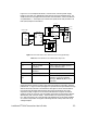
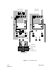
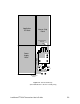
onto the network wiring. The physical placement of Z1 and Z2 should be near the
entry points of the network wiring with a low impedance path to chassis ground (or
alternately to star ground near star ground center). The external components for
figure 2.2 are shown in table 2.4.
NET_A
NET_B
VCC
T1
T2
GND
RXD
TXD
CLK
FTT-10A
CP0
CP1
CLK2
CP2
CP3
CP4
Neuron Chip
(Partial)
+5V
+5V
D1
NET1
NET2
See Text
D2
D3
D4
C3
C1
C4
D5
D6
C2
Z1 Z2
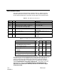
Figure 2.2 FTT-10A Transceiver Interconnection Without Spark Gaps
Table 2.4 FTT-10A Transceiver External Components
Name Value Comments
C1 0.1µF for +5VDC decoupling Power supply decoupling capacitor
for FTT-10A transceiver
C2 1000pF, 2kV, Low inductance ESD snubber capacitor
C3,C4 22µF, +50V, polar DC blocking capacitors; see text
D1, D2 BAV99 or 1N4148(x2) Transient clamping diodes;
BAV99LT1 (National), BAV99LT
(Sprague), MMBD120 (Motorola), or
equivalent
D3, D4, D5, D6 1N4934, 1N4935, or Motorola
SMT version MRA4935T3
Fast switching rectifiers (General
Instruments or Motorola)
Z1, Z2 DSP-301N Fast surge protectors with microgap
(source: Mitsubishi Materials
Corporation at US phone number
+1-847-577-0200, or fax number
+1-847-577-0201 or Europe
(London) phone +44-171-236-0130)
Some applications require compliance only with Level 4 of the preferred contact-
discharge method for electrostatic discharge (ESD) as defined in IEC 1000-4-2. For
these applications, diodes D3 and D4, and capacitor C2, as shown in figure 2.1, can
be deleted. This simplified circuit has been tested at Level 4 under the preferred