InvenSense Inc. 1197 Borregas Ave, Sunnyvale, CA 94089 U.S.A. Tel: +1 (408) 988-7339 Fax: +1 (408) 988-8104 Website: www.invensense.com Document Number: PS-ITG-3200A-00-01.4 Revision: 1.4 Release Date: 03/30/2010 ITG-3200 Product Specification Revision 1.
ITG-3200 Product Specification Document Number: PS-ITG-3200A-00-01.4 Revision: 1.4 Release Date: 03/30/2010 CONTENTS 1 DOCUMENT INFORMATION .............................................................................................................................. 4 1.1 1.2 1.3 1.4 REVISION HISTORY ............................................................................................................................................. 4 PURPOSE AND SCOPE ............................................
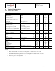
ITG-3200 Product Specification 9.5 9.6 9.7 9.8 9.9 9.10 9.11 9.12 9.13 10 10.1 10.2 Document Number: PS-ITG-3200A-00-01.4 Revision: 1.4 Release Date: 03/30/2010 LABEL ................................................................................................................................................................33 PACKAGING ........................................................................................................................................................
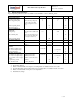
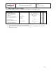
ITG-3200 Product Specification 1 Document Number: PS-ITG-3200A-00-01.4 Revision: 1.4 Release Date: 03/30/2010 Document Information 1.1 Revision History Revision Date Revision 10/23/09 1.0 Initial Release 10/28/09 1.1 02/12/2010 1.2 Edits for readability Changed full-scale range and sensitivity scale factor (Sections 2, 3.1, 5.3, and 8.3) Changed sensitivity scale factor variation over temperature (Section 3.1) Changed total RMS noise spec (Section 3.
ITG-3200 Product Specification Document Number: PS-ITG-3200A-00-01.4 Revision: 1.4 Release Date: 03/30/2010 1.2 Purpose and Scope This document is a preliminary product specification, providing a description, specifications, and design related information for the ITG-3200TM. Electrical characteristics are based upon simulation results and limited characterization data of advanced samples only. Specifications are subject to change without notice.
ITG-3200 Product Specification 2 Document Number: PS-ITG-3200A-00-01.4 Revision: 1.4 Release Date: 03/30/2010 Features The ITG-3200 triple-axis MEMS gyroscope includes a wide range of features: Digital-output X-, Y-, and Z-Axis angular rate sensors (gyros) on one integrated circuit with a sensitivity of 14.
Document Number: PS-ITG-3200A-00-01.4 Revision: 1.4 Release Date: 03/30/2010 ITG-3200 Product Specification 3 Electrical Characteristics 3.1 Sensor Specifications Typical Operating Circuit of Section 4.2, VDD = 2.5V, VLOGIC = 1.71V to VDD, TA=25°C.
Document Number: PS-ITG-3200A-00-01.4 Revision: 1.4 Release Date: 03/30/2010 ITG-3200 Product Specification 3.2 Electrical Specifications Typical Operating Circuit of Section 4.2, VDD = 2.5V, VLOGIC = 1.71V to VDD, TA=25°C. Parameters VDD POWER SUPPLY Operating Voltage Range Power-Supply Ramp Rate Conditions Monotonic ramp. Ramp rate is 10% to 90% of the final value (see Figure in Section 4.4) Min 2.
Document Number: PS-ITG-3200A-00-01.4 Revision: 1.4 Release Date: 03/30/2010 ITG-3200 Product Specification 3.3 Electrical Specifications, continued Typical Operating Circuit of Section 4.2, VDD = 2.5V, VLOGIC = 1.71V to VDD, T A=25°C.
Document Number: PS-ITG-3200A-00-01.4 Revision: 1.4 Release Date: 03/30/2010 ITG-3200 Product Specification 3.4 Electrical Specifications, continued Typical Operating Circuit of Section 4.2, VDD = 2.5V, VLOGIC = 1.71V to VDD, TA=25°C.
Document Number: PS-ITG-3200A-00-01.4 Revision: 1.4 Release Date: 03/30/2010 ITG-3200 Product Specification 2 3.5 I C Timing Characterization Typical Operating Circuit of Section 4.2, VDD = 2.5V, VLOGIC = 1.8V±5%, 2.5V±5%, 3.0V±5%, or 3.3V±5%, TA=25°C. Parameters I2C TIMING fSCL, SCL Clock Frequency Conditions I2C FAST-MODE Min 0 Typical Max Units Notes 400 kHz 1 tHD.STA, (Repeated) START Condition Hold Time 0.6 us 1 tLOW, SCL Low Period 1.3 us 1 tHIGH, SCL High Period 0.6 us 1 tSU.
ITG-3200 Product Specification 3.6 Document Number: PS-ITG-3200A-00-01.4 Revision: 1.4 Release Date: 03/30/2010 Absolute Maximum Ratings Stresses above those listed as “Absolute Maximum Ratings” may cause permanent damage to the device. These are stress ratings only and functional operation of the device at these conditions is not implied. Exposure to the absolute maximum ratings conditions for extended periods may affect device reliability.
ITG-3200 Product Specification 4 Document Number: PS-ITG-3200A-00-01.4 Revision: 1.4 Release Date: 03/30/2010 Applications Information 4.1 Pin Out and Signal Description Number Pin Pin Description 1 CLKIN 8 VLOGIC Optional external reference clock input. Connect to GND if unused. 9 AD0 10 REGOUT 12 INT Interrupt digital output (totem pole or open-drain) 13 VDD Power supply voltage 18 GND Power supply ground Digital IO supply voltage. VLOGIC must be ≤ VDD at all times.
Document Number: PS-ITG-3200A-00-01.4 Revision: 1.4 Release Date: 03/30/2010 ITG-3200 Product Specification 4.2 Typical Operating Circuit SDA SCL CLKIN 24 23 GND C1 2.2nF 22 21 20 19 1 18 2 17 3 16 GND ITG-3200 4 15 VDD 5 14 6 13 7 8 9 10 11 12 C2 0.1µF VLOGIC GND GND INT C3 0.1µF AD0 C4 10nF GND GND Typical Operating Circuit 4.3 Bill of Materials for External Components Component Label Specification Quantity Charge Pump Capacitor C1 Ceramic, X7R, 2.
ITG-3200 Product Specification Recommended Power-On Procedure All Voltages at 0V 4.4 Document Number: PS-ITG-3200A-00-01.4 Revision: 1.4 Release Date: 03/30/2010 Power-Up Sequencing 1. TVDDR is VDD rise time: Time for VDD to rise from 10% to 90% of its final value TVDDR 2. TVDDR is ≤5msec 90% VDD 3. TVLGR is VLOGIC rise time: Time for VLOGIC to rise from 10% to 90% of its final value 10% TVLGR 90% VLOGIC 10% TVLG - VDD 4. TVLGR is ≤1msec 5.
ITG-3200 Product Specification 5 5.1 Document Number: PS-ITG-3200A-00-01.4 Revision: 1.
ITG-3200 Product Specification Document Number: PS-ITG-3200A-00-01.4 Revision: 1.4 Release Date: 03/30/2010 2 5.4 I C Serial Communications Interface The ITG-3200 communicates to a system processor using the I2C serial interface, and the device always acts as a slave when communicating to the system processor. The logic level for communications to the master is set by the voltage on the VLOGIC pin. The LSB of the of the I2C slave address is set by pin 9 (AD0). 5.
ITG-3200 Product Specification 6 Document Number: PS-ITG-3200A-00-01.4 Revision: 1.4 Release Date: 03/30/2010 Digital Interface 2 6.1 I C Serial Interface The internal registers and memory of the ITG-3200 can be accessed using I2C at up to 400kHz. Serial Interface Pin Number Pin Name Pin Description 8 VLOGIC Digital IO supply voltage. VLOGIC must be ≤ VDD at all times. 9 AD0 I2C Slave Address LSB 23 SCL I2C serial clock 24 SDA I2C serial data 2 6.1.
ITG-3200 Product Specification Document Number: PS-ITG-3200A-00-01.4 Revision: 1.4 Release Date: 03/30/2010 Data Format / Acknowledge I2C data bytes are defined to be 8 bits long. There is no restriction to the number of bytes transmitted per data transfer. Each byte transferred must be followed by an acknowledge (ACK) signal.
Document Number: PS-ITG-3200A-00-01.4 Revision: 1.4 Release Date: 03/30/2010 ITG-3200 Product Specification To write the internal ITG-3200 device registers, the master transmits the start condition (S), followed by the I2C address and the write bit (0). At the 9th clock cycle (when the clock is high), the ITG-3200 device acknowledges the transfer. Then the master puts the register address (RA) on the bus.
ITG-3200 Product Specification Document Number: PS-ITG-3200A-00-01.4 Revision: 1.
Document Number: PS-ITG-3200A-00-01.4 Revision: 1.
Document Number: PS-ITG-3200A-00-01.4 Revision: 1.4 Release Date: 03/30/2010 ITG-3200 Product Specification 8 Register Description This section details each register within the InvenSense ITG-3200 gyroscope. Note that any bit that is not defined should be set to zero in order to be compatible with future InvenSense devices. The register space allows single-byte reads and writes, as well as burst reads and writes.
Document Number: PS-ITG-3200A-00-01.4 Revision: 1.4 Release Date: 03/30/2010 ITG-3200 Product Specification 8.3 Register 22 – DLPF, Full Scale Type: Read/Write Register (Hex) 16 Register (Decimal) 22 Bit7 Bit6 Bit5 - Bit4 Bit3 Bit2 FS_SEL Bit1 Bit0 DLPF_CFG Default Value 00h Description: This register configures several parameters related to the sensor acquisition. The FS_SEL parameter allows setting the full-scale range of the gyro sensors, as described in the table below.
Document Number: PS-ITG-3200A-00-01.4 Revision: 1.4 Release Date: 03/30/2010 ITG-3200 Product Specification DLPF Characteristics: The gain and phase responses of the digital low pass filter settings (DLPF_CFG) are shown below: Bode Diagram Magnitude (dB) 0 -10 6 5 4 3 21 0 -20 -30 -40 -50 Phase (deg) 0 -45 6 5 4 3 2 1 0 -90 0 1 10 2 10 3 10 10 Frequency (Hz) Gain and Phase vs.
Document Number: PS-ITG-3200A-00-01.4 Revision: 1.4 Release Date: 03/30/2010 ITG-3200 Product Specification 8.4 Register 23 – Interrupt Configuration Type: Read/Write Register (Hex) Register (Decimal) Bit7 Bit6 Bit5 Bit4 Bit3 Bit2 Bit1 Bit0 Default Value 17 23 ACTL OPEN LATCH_ INT_EN INT_ ANYRD_ 2CLEAR 0 ITG_RDY_ EN 0 RAW_ RDY_ EN 00h Description: This register configures the interrupt operation of the device.
Document Number: PS-ITG-3200A-00-01.4 Revision: 1.4 Release Date: 03/30/2010 ITG-3200 Product Specification 8.6 Registers 27 to 34 – Sensor Registers Type: Read only Register (Hex) Register (Decimal) 1B 1C 1D 1E 1F 20 21 22 27 28 29 30 31 32 33 34 Bit7 Bit6 Bit5 Bit4 Bit3 Bit2 Bit1 Bit0 TEMP_OUT_H TEMP_OUT_L GYRO_XOUT_H GYRO_XOUT_L GYRO_YOUT_H GYRO_YOUT_L GYRO_ZOUT_H GYRO_ZOUT_L Description: These registers contain the gyro and temperature sensor data for the ITG-3200 parts.
ITG-3200 Product Specification Parameters: H_RESET SLEEP STBY_XG STBY_YG STBY_ZG CLK_SEL Document Number: PS-ITG-3200A-00-01.4 Revision: 1.
Document Number: PS-ITG-3200A-00-01.4 Revision: 1.4 Release Date: 03/30/2010 ITG-3200 Product Specification 9 9.1 Assembly Orientation The diagram below shows the orientation of the axes of sensitivity and the polarity of rotation.
ITG-3200 Product Specification 9.2 Document Number: PS-ITG-3200A-00-01.4 Revision: 1.
Document Number: PS-ITG-3200A-00-01.4 Revision: 1.4 Release Date: 03/30/2010 ITG-3200 Product Specification 9.3 Package Marking Specification TOP VIEW InvenSense ITG-3200 XXXXXX-XX XX YYWW X Part number Lot traceability code Foundry code Package Vendor Code Rev Code YY = Year Code WW = Work Week Package Marking Specification 9.
Document Number: PS-ITG-3200A-00-01.4 Revision: 1.4 Release Date: 03/30/2010 ITG-3200 Product Specification Reel Outline Drawing Reel Dimensions and Package Size REEL (mm) PKG SIZE L V W Z 4x4 330 100 13.2 2.
ITG-3200 Product Specification 9.5 Document Number: PS-ITG-3200A-00-01.4 Revision: 1.4 Release Date: 03/30/2010 Label Location of Label 9.
Document Number: PS-ITG-3200A-00-01.4 Revision: 1.4 Release Date: 03/30/2010 ITG-3200 Product Specification 9.7 Soldering Exposed Die Pad The ITG-3200 has very low active and standby current consumption. The exposed die pad is not required for heat sinking, and should not be soldered to the PCB since soldering to it contributes to performance changes due to package thermo-mechanical stress. 9.
ITG-3200 Product Specification 9.10 Document Number: PS-ITG-3200A-00-01.4 Revision: 1.4 Release Date: 03/30/2010 MEMS Handling Instructions MEMS (Micro Electro-Mechanical Systems) are a time-proven, robust technology used in hundreds of millions of consumer, automotive and industrial products. MEMS devices consist of microscopic moving mechanical structures. They differ from conventional IC products even though they can be found in similar packages.
ITG-3200 Product Specification Document Number: PS-ITG-3200A-00-01.4 Revision: 1.
ITG-3200 Product Specification Document Number: PS-ITG-3200A-00-01.4 Revision: 1.4 Release Date: 03/30/2010 9.13 Storage Specifications The storage specification of the ITG-3200 gyroscope conforms to IPC/JEDEC J-STD-020C Moisture Sensitivity Level (MSL) 3.
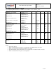
ITG-3200 Product Specification Document Number: PS-ITG-3200A-00-01.4 Revision: 1.4 Release Date: 03/30/2010 10 Reliability 10.1 Qualification Test Policy InvenSense’s products complete a Qualification Test Plan before being released to production. The Qualification Test Plan follows the JEDEC 47D Standards, “Stress-Test-Driven Qualification of Integrated Circuits,” with the individual tests described below. 10.
ITG-3200 Product Specification Document Number: PS-ITG-3200A-00-01.4 Revision: 1.4 Release Date: 03/30/2010 This information furnished by InvenSense is believed to be accurate and reliable. However, no responsibility is assumed by InvenSense for its use, or for any infringements of patents or other rights of third parties that may result from its use. Specifications are subject to change without notice.