
Data Sheet

ITG-3200 Product Specification
Document Number: PS-ITG-3200A-00-01.4
Revision: 1.4
Release Date: 03/30/2010
11 of 39
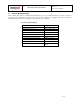
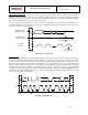
3.5 I
2
C Timing Characterization
Typical Operating Circuit of Section 4.2, VDD = 2.5V, VLOGIC = 1.8V±5%, 2.5V±5%, 3.0V±5%, or 3.3V±5%,
T
A
=25°C.
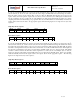
Parameters
Conditions
Min
Typical
Max
Units
Notes
I
2
C TIMING
I
2
C FAST-MODE
f
SCL
, SCL Clock Frequency
0
400
kHz
1
t
HD.STA
, (Repeated) START Condition Hold Time
0.6
us
1
t
LOW
, SCL Low Period
1.3
us
1
t
HIGH
, SCL High Period
0.6
us
1
t
SU.STA
, Repeated START Condition Setup Time
0.6
us
1
t
HD.DAT
, SDA Data Hold Time
0
us
1
t
SU.DAT
, SDA Data Setup Time
100
ns
1
t
r
, SDA and SCL Rise Time
Cb bus cap. from 10 to 400pF
20+0.1Cb
300
ns
1
t
f
, SDA and SCL Fall Time
Cb bus cap. from 10 to 400pF
20+0.1Cb
300
ns
1
t
SU.STO
, STOP Condition Setup Time
0.6
us
1
t
BUF
, Bus Free Time Between STOP and START
Condition
1.3
us
1
C
b
, Capacitive Load for each Bus Line
400
pF
2
t
VD.DAT
, Data Valid Time
0.9
us
1
t
VD.ACK
, Data Valid Acknowledge Time
0.9
us
1
Notes:
1. Based on characterization of 5 pieces over temperature on evaluation board or in socket
2. Guaranteed by design
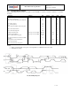
I
2
C Bus Timing Diagram