
Data Sheet

ITG-3200 Product Specification
Document Number: PS-ITG-3200A-00-01.4
Revision: 1.4
Release Date: 03/30/2010
13 of 39
4 Applications Information
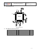
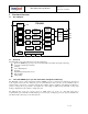
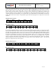
4.1 Pin Out and Signal Description
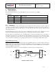
Number
Pin
Pin Description
1
CLKIN
Optional external reference clock input. Connect to GND if unused.
8
VLOGIC
Digital IO supply voltage. VLOGIC must be ≤ VDD at all times.
9
AD0
I
2
C Slave Address LSB
10
REGOUT
Regulator filter capacitor connection
12
INT
Interrupt digital output (totem pole or open-drain)
13
VDD
Power supply voltage
18
GND
Power supply ground
11
RESV-G
Reserved - Connect to ground.
6, 7, 19, 21, 22
RESV
Reserved. Do not connect.
20
CPOUT
Charge pump capacitor connection
23
SCL
I
2
C serial clock
24
SDA
I
2
C serial data
2, 3, 4, 5, 14, 15, 16, 17
NC
Not internally connected. May be used for PCB trace routing.
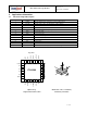
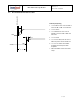
ITG
-
3200
+Z
+X
+Y
7 8 9 10 11 12
RESV
VLOGIC
AD0
REGOUT
RESV-G
INT
13
18
17
16
15
14
NC
NC
NC
VDD
NC
GND
6
1
2
3
4
5
NC
NC
NC
RESV
NC
CLKIN
24 23 22 21 20 19
RESV
CPOUT
RESV
RESV
SCL
SDA
ITG-3200
QFN Package
24-pin, 4mm x 4mm x 0.9mm
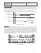
Orientation of Axes of Sensitivity
and Polarity of Rotation
Top View