
Data Sheet

ITG-3200 Product Specification
Document Number: PS-ITG-3200A-00-01.4
Revision: 1.4
Release Date: 03/30/2010
8 of 39
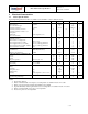
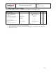
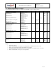
3.2 Electrical Specifications
Typical Operating Circuit of Section 4.2, VDD = 2.5V, VLOGIC = 1.71V to VDD, T
A
=25°C.
Parameters
Conditions
Min
Typical
Max
Units
Notes
VDD POWER SUPPLY
Operating Voltage Range
2.1
3.6
V
2
Power-Supply Ramp Rate
Monotonic ramp. Ramp rate
is 10% to 90% of the final
value (see Figure in Section
4.4)
0
5
ms
2
Normal Operating Current
6.5
mA
1
Sleep Mode Current
5
µA
5
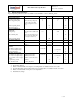
VLOGIC REFERENCE
VOLTAGE
Voltage Range
VLOGIC must be ≤VDD at all
times
1.71
VDD
V
VLOGIC Ramp Rate
Monotonic ramp. Ramp rate is
10% to 90% of the final value
(see Figure in Section 4.4)
1
ms
6
Normal Operating Current
100
µA
START-UP TIME FOR
REGISTER READ/WRITE
20
ms
5
I
2
C ADDRESS
AD0 = 0
1101000
6
AD0 = 1
1101001
6
DIGITAL INPUTS (AD0,
CLKIN)
V
IH
, High Level Input Voltage
0.9*VLOGIC
V
5
V
IL
, Low Level Input Voltage
0.1*VLOGIC
V
5
C
I
, Input Capacitance
5
pF
7
DIGITAL OUTPUT (INT)
V
OH
, High Level Output Voltage
OPEN=0, Rload=1MΩ
0.9*VLOGIC
V
2
V
OL
, Low Level Output Voltage
OPEN=0, Rload=1MΩ
0.1*VLOGIC
V
2
V
OL.INT1
, INT Low-Level Output
Voltage
OPEN=1, 0.3mA sink current
0.1
V
2
Output Leakage Current
OPEN=1
100
nA
4
t
INT
, INT Pulse Width
LATCH_INT_EN=0
50
µs
4
Notes:
1. Tested in production
2. Based on characterization of 30 pieces over temperature on evaluation board or in socket
4. Typical. Randomly selected part measured at room temperature on evaluation board or in socket
5. Based on characterization of 5 pieces over temperature
6. Guaranteed by design