
Data Sheet


PN512_C1_SDS All information provided in this document is subject to legal disclaimers. © NXP B.V. 2012. All rights reserved.
Product short data sheet
COMPANY PUBLIC
Rev. 3.2 — 20 September 2012
120132 3 of 27
NXP Semiconductors
PN532/C1
Near Field Communication (NFC) controller
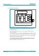
Power switch for external secure companion chip
Dedicated IO ports for external device control
Integrated antenna detector for production tests
ECMA 373 NFC-WI interface to connect an external secure IC
3. Applications
Mobile and portable devices
Consumer applications
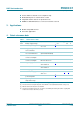
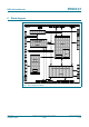
4. Quick reference data
[1] DV
DD
, AV
DD
and TV
DD
must always be at the same supply voltage.
[2] The total current consumption depends on the firmware version (different internal IC clock speed)
[3] With an antenna tuned at 50 at 13.56 MHz
[4] The antenna should be tuned not to exceed this current limit (the detuning effect when coupling with
another device must be taken into account)
Table 1. Quick reference data
Symbol Parameter Conditions Min Typ Max Unit
V
BAT
Battery supply voltage 2.7 5.5 V
ICV
DD
LDO output voltage V
BAT
>3.4V
V
SS
=0V
[1]
2.7 3 3.4 V
PV
DD
Supply voltage
for host interface
V
SS
= 0 V 1.6 - 3.6 V
SV
DD
Output voltage
for secure IC interface
V
SS
= 0 V
(SV
DD
Switch Enabled)
DV
DD
-0.5 - DV
DD
V
I
HPD
Hard-Power-Down
current consumption
V
BAT
=5V - - 2 A
I
SPD
Soft-Power-Down
current consumption
V
BAT
= 5 V,
RF level detector on
--45A
I
DVDD
Digital supply current V
BAT
=5 V,
SV
DD
switch off
[1]
-25-mA
I
SVDD
SV
DD
load current V
BAT
=5V,
SV
DD
switch on
--30mA
I
AVDD
Analog supply current V
BAT
=5 V - 6 - mA
I
TVDD
Transmitter supply current During RF transmission,
V
BAT
=5 V
-60
[3]
150
[4]
mA
P
tot
Continuous total
power dissipation
T
amb
=-30to+85C
[2]
--0.5W
T
amb
Operating
temperature range
-30 - +85 C