
Datasheet


EA DIP240-7
Page 2
ELECTRONIC ASSEMBLY reserves
the right to change specifications
without prior notice. Printing and
typographical errors reserved.
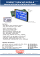
LC-GRAPHIC DISPLAY EA DIP240-7
The very successful display line from ELECTRONIC ASSEMBLY, called DIP-series get's with it's
EA P240-7 a new memer now. Simple placing and soldering into pcb will manage not even electrical
contact but also mechanical mounting.
The displays EA DIP240-7 provide a full graphic resolution of 240x128 dots and are at once all
advantages of modern displays: standard controller T6963 on-board, fashionable LED- backlight with
blue optic, single supply +5V, no additional power supply is required, wide operating temperature
range incl. built-in temperature compensation.
LED BACKLIGHT
Both types are equipped wit a white LED-backlight. Please note that LEDs are wearable parts. Life
time is between 1,000 and 20,000 hours
*)
, depending from ambient conditions. A current limiting
resistor for max. 120mA is built-in already. Please take into account a derating for temeratures higher
than >+25°C. To extend life time backlight can be switched on and off directly via processor port (pin
LEDoff)
. Life time can be increase by reduction of driving current, too.
CONTROLLER T6963C BUILT-IN
All modules provide a built-in T6963C. Therefore a direct interface to 8-Bit processor system is
available together with a comfortable command set. With that there's a complete caracter set built-in
for example. This can be extended or completely exchanged by some self-definable characters, too.
Every single character may be advised by a, attribute like "invers", "blink" or "invisible".
More than 8 pages are available even in graphic mode (32kB). Text can be joined via "and-", "or-",
"exor-" function with graphics layer.
CONTRAST ADJUSTMENT
Contrast pre-adjusted ex works. Thanks to the integrated temperature compensation there's no need
to adjust while operation anymore.
Is contrast adjustment requested nevertheless, an external potentiometer need to be
connected and SMD potentiometer RV1 has to be desoldered. For external circuit please
follow the schematic at the right.
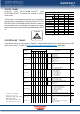
PINOUT
Pin Symbol Function Pin Symbol Function
1 N.C.
Do not connect
21 GND Ground Potential for logic (0V)
2 N.C. 22 VDD Power supply for logic (+5V)
3 N.C. 23 RV Operating voltage for LC driving (input)
4 N.C. 24 VEE Output voltage for LC driving
5 N.C. 25 C/D L: Data input H: Command input
6 N.C. 26 WR L: Data Write
7 N.C. 27 RD L: Data Read
8 N.C. 28 CE L: Chip Enable
9 N.C. 29 RST L: Reset
10 N.C. 30 DB0 Data Bus Line, LSB
11 N.C. 31 DB1 Data Bus Line
12 N.C. 32 DB2 Data Bus Line
13 N.C. 33 DB3 Data Bus Line
14 N.C. 34 DB4 Data Bus Line
15 N.C. 35 DB5 Data Bus Line
16 N.C. 36 DB6 Data Bus Line
17 BOTTOM Touch Panel 37 DB7 Data Bus Line, MSB
18 LEFT Touch Panel 38 LEDoff L: LED off; Pull-up 100k built-in
19 TOP Touch Panel 39 A LED backlight Anode +5V
20 RIGHT Touch Panel 40 C LED backlight Cathode 0V
*)
Prior art