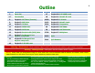
Outline Page # 3 4-7 Title Page # Title Parts List 17 Project 10: S-R NAND Latch Introduction 18 Project 11: Gated S-R Latch 8 Project 1: NOT Gate (Inverter) 19-20 Project 12: J-K Latch 9 Project 2: AND Gate 21-22 Project 13: Gated D Latch 10 Project 3: OR Gate 23-24 Project 14: Comparator 11 Project 4: NAND Gate 25 Project 15: Half Adder 12 Project 5: NOR Gate 26 Project 16: Half Subtractor 13 Project 6: Exclusive OR (XOR) Gate 14 Project 7: De Morgan’s Law Negation of C
Parts List ID 1 2 3 4 5 6 7 B1 D1 D2 R2 S1 U15 U16 U17 U18 U19 U20 Part Name 1-snap wire 2-snap wire 3-snap wire 4-snap wire 5-snap wire 6-snap wire 7-snap wire Battery Holder 4.5V (3-AA) Base Grid (11.0” x 7.
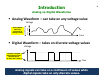
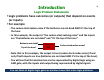
Introduction Analog vs. Digital Waveforms Analog Waveform – can take on any voltage value Voltage Analog Signal takes on a Continuum of Voltage values 5 4 3 2 1 0 Time Digital Waveform – takes on discrete voltage values Voltage 5 Example of Digital Signal taking on two discrete values (0 Volts and 5 Volts) 0 Time Analog signals can take on a continuum of values while digital signals take on only discrete values.
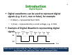
Introduction Digital Signals Digital waveforms can be used to represent digital signals (e.g. 0 or 1, true or false), for example • 0 (false) – represented by 0 Volts • 1 (true) – represented by a small voltage, e.g. 3 Volts Example of Digital Waveform representing digital signals True False False True False True True False 1 0 0 1 0 1 1 0 3V 0V Time Digital signals are represented by a “high” state (1) or “true” state consisting of a small voltage (e.g.
Introduction 6 Logic Problem Statements Logic problems have outcomes (or outputs) that depend on events (or inputs). For example • The cuckoo clock makes noise if the batteries are not dead AND it’s the top of the hour. • In this example, the output is “the cuckoo clock making noise” and the inputs are “the batteries are not dead” and “it’s the top of the hour”.
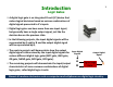
Introduction Logic Gates A digital logic gate is an Integrated Circuit (IC) device that makes logical decisions based on various combinations of digital signals presented to it’s inputs. Digital logic gates can have more than one input signal, but generally have a single output signal, just like the decision box on the previous slide. In the following projects, the input digital signals will be represented by A and/or B and the output digital signal will be represented by Q.
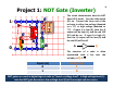
Project 1: NOT Gate (Inverter) 2 3 1 1 2 A 2 U15 1 Q 1 1 2 3 1 2 This circuit demonstrates how the NOT Gate (U15) works. Turn the slide switch (S1) on. Connect the loose end of the red wire to either low voltage (denoted as a “0”) or high voltage (denoted as “1”). If input A is low (0), then the Q output will be high (1), and the red LED (D1) will be on. If input A is high (1), then the Q output will be low (0) and the red LED will be off.
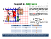
Project 2: AND Gate This circuit demonstrates how the AND Gate (U16) works. Turn the slide switch (S1) on. Connect the loose ends of the red and black wires to either low voltage (denoted as a “0”) or high voltage (denoted as a “1”). If, and only if, both input A AND input B are high (both 1s), then the Q output will be high (1), and the red LED (D1) will be on.
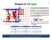
Project 3: OR Gate 2 1 This circuit demonstrates how the OR Gate (U17) works. Turn the slide switch (S1) on. Connect the loose ends of the red and black wires to either low voltage (denoted as a “0”) or high voltage (denoted as a “1”). If either input A OR input B are high (1), then the Q output will be high (1), and the red LED (D1) will be on. 3 1 A 2 2 1 U17 B 2 3 1 1 2 Q2 1 A B 2 0 1 2 2 Q The output of an OR gate is often represented as the sum of the inputs, so Q = A+B.
Project 4: NAND Gate This circuit demonstrates how the NAND Gate (U18) works. Turn the slide switch (S1) on. Connect the loose ends of the red and black wires to either low voltage (denoted as a “0”) or high voltage (denoted as a “1”). If either input A OR input B are low (0), then the Q output on U18 will be high (1), and the red LED (D1) will be on. The output logic is exactly the opposite of the AND gate, hence this gate is called the NOT AND or NAND Gate.
Project 5: NOR Gate This circuit demonstrates how the NOR Gate (U19) works. Turn the slide switch (S1) on. Connect the loose ends of the red and black wires to either low voltage (denoted as a “0”) or high voltage (denoted as a “1”). If, and only if, both input A AND input B are low (0), then the Q output on U19 will be high (1), and the red LED (D1) will be on. The output logic is exactly the opposite of the OR gate, hence this gate is called the NOT OR or NOR Gate.
Project 6: Exclusive OR (XOR) Gate 2 1 This circuit demonstrates how the Exclusive OR (XOR) Gate (U20) works. Turn the slide switch (S1) on. Connect the loose ends of the red and black wires to either low voltage (denoted as a “0”) or high voltage (denoted as a “1”). If input A and input B are exclusive (i.e. different), then the Q output on U20 will be high (1), and the red LED (D1) will be on.
Project 7: De Morgan’s Law Negation of Conjunction 1 1 3 2 U15 2 2 U15 4 2 B 1 3 Q 2 2 1 4 A 4 U15 2 2 2 2 1 0 3 2 2 1 3 1 2 1 2 3 2 A B 5 1 U16 3 1 2 2 1 2 U17 3 1 2 3 2 3 3 2 2 1 2 This circuit demonstrates De Morgan’s Law of Negation of Conjunction which states that the negation of a conjunction is equivalent to disjunction of the negations. Turn the slide switch (S1) on.
Project 8: De Morgan’s Law Negation of Disjunction 3 1 3 2 U15 2 2 U15 4 2 B 2 1 3 Q 2 2 1 4 2 A 4 U15 2 2 2 2 1 0 3 2 1 3 1 2 1 2 3 2 A B 5 1 U17 3 1 2 2 1 2 U16 3 1 3 3 2 3 1 2 2 1 2 This circuit demonstrates De Morgan’s Law of Negation of Disjunction which states that the negation of a disjunction is equivalent to conjunction of the negations. Turn the slide switch (S1) on.
Project 9: S-R NOR Latch 1 1 2 2 1 2 2 2 3 3 U19 2 S 2 Input (S) 2 1 0 1 2 3 4 2 1 2 U19 1 2 Q 1 Input (R) R 2 1 2 1 This circuit demonstrates how the S-R NOR Latch works. Turn the slide switch (S1) on. Connect the loose end of the red wire (S input) to 0 and the loose end of the black wire (R input) to 1. The red LED will be off (S=0, R=1 resets output Q to 0). Now disconnect the black wire from 1 and connect it to 0.
Project 10: S-R NAND Latch 1 1 2 2 0 1 2 2 2 3 3 U18 1 S 2 1 2 1 3 2 4 2 1 2 U18 2 2 Q 1 R 2 1 1 2 Q This circuit demonstrates how the S-R NAND Latch works. Turn the slide switch (S1) on. Connect the loose end of the red wire (S input) to 1 and the loose end of the black wire (R input) to 0. The red LED will be off (S=1, R=0 resets output Q to 0). Now disconnect the black wire from 0 and connect it to 1. The red LED remains off (S=1, R=1 holds the last output state).
Project 11: Gated S-R Latch 1 1 2 2 3 2 1 1 S 2 0 3 2 2 3 2 U19 2 1 1 2 3 2 U19 1 2 2 3 1 U16 4 2 2 1 2 2 2 Q 3 3 2 Q 0 4 2 2 R 1 3 3 E U16 2 2 3 Input (E) Q, Q 0 Hold State 1 Same as S-R Latch 1 1 18 This circuit demonstrates how a Gated S-R Latch works. Turn the slide switch (S1) on. Connect one the loose end of the orange wire to 1 (Latch enabled). Repeat the experiments from Project 9 to verify that this now functions as an S-R NOR Latch.
Project 12: J-K Latch 2 1 2 2 3 2 1 4 U16 2 U19 2 2 Q 2 U16 2 2 K 3 2 3 4 2 2 2 3 0 4 1 U19 2 4 2 3 2 1 2 2 2 1 2 1 3 1 J 1 3 3 2 1 Q 1 19 This circuit demonstrates how a J-K Latch works. Turn the slide switch (S1) on. Connect the loose ends of the red and black jumper wires to either 0 or 1.
Project 12: J-K Latch K J 1 2 4 Q 3 Q Stays the same when J=K=0 Reset to 0 when J=0 & K=1 Set to 1 when J=1 & K=0 Toggles when J=K=1 Input (J) Input (K) Output (Q) Output (Q) 0 0 Hold State Hold State 1 0 1 0 0 1 0 1 1 1 Toggle Toggle J-K Latches and flip flops are used for memory devices and counters.
Project 13: Gated D Latch 3 2 1 3 U19 3 2 1 3 3 3 2 0 2 2 3 1 2 3 1 U19 2 2 2 1 2 2 2 2 4 U16 D 2 4 U15 1 3 Q 2 5 2 1 4 3 2 2 2 2 3 2 2 E 2 1 1 U16 2 3 2 2 4 1 1 21 3 2 1 Q This circuit demonstrates how a Gated D Latch works. Turn the slide switch (S1) on.
Project 13: Gated D Latch D 5 1 4 Q 3 Q Stays the same when E=0 Reset to 0 when D=0 & E=1 Set to 1 when D=1 & E=1 E 2 E D Output (Q) Output (Q) 0 0 or 1 Hold State Hold State 1 0 0 1 1 1 1 0 The Gated D Latch exploits the fact that the active input combinations on an S-R Latch (S=1, R=0 and S=0, R=1) produce opposite outputs. Thus, the Gated D Latch can be thought of as a single input Gated S-R Latch. Gated D Latches can be used as Input/Output (I/O) ports.
Project 14: Comparator 2 1 2 2 3 2 1 1 1 U15 3 3 U16 2 1 3 1 4 2 A 2 2 2 2 2 1 3 1 2 2 1 2 2 3 2 2 0 3 1 3 1 2 1 2 2 3 B U19 U16 U15 2 3 2 2 5 2 1 2 Q This circuit demonstrates how a comparator works. Turn the slide switch (S1) on. When the loose ends of the red and black wires are connected to the same input (either 1 or 0), the red LED will be on (indicating the inputs are the same).
Project 14: Comparator A 1 Equal to 1 when A=B Equals 0 when A ≠ B 4 Q 5 B 2 Simpler Comparator Circuit 3 A B Q A B Output (Q) 0 0 1 0 1 0 1 0 0 1 1 1 Comparators are used in Central Processing Units (CPUs) and Microcontrollers (MCUs).
Project 15: Half Adder 1 1 2 2 2 U20 U16 1 1 1 2 1 2 2 2 S 1 2 B 1 2 3 2 C A 32 2 2 2 4 3 1 This circuit demonstrates how a half adder works. Turn the slide switch (S1) on. The green LED represents the Sum (S) and the red LED represents the Carry (C). When the loose ends of the red and black wires are both connected to 0 (0+0), both LEDs are off (S=C=0).
Project 16: Half Subtractor 1 2 2 1 2 U20 1 2 1 2 This circuit demonstrates how a half subtractor works. Turn the slide switch (S1) on. The green LED represents the Difference (D) of input A minus input B and the red LED represents the Borrow (B). When the loose ends of the red and black wires are both connected to 0 (0-0) or to 1 (1-1), both LEDs are off (D=B=0).
Project 17: Multiplexer 2 1 2 2 3 3 2 1 1 U15 3 U16 1 2 1 2 4 B 2 2 1 3 1 1 3 2 0 2 U17 2 3 1 2 3 U16 2 A 2 2 1 2 3 2 2 2 2 1 3 2 2 1 This circuit demonstrates how a multiplexer works. Turn the slide switch (S1) on. The loose end of the orange wire represents the Selector (S). First connect the loose end of the orange wire to 1 (this selects the black input).
Project 17: Multiplexer A S represents the Selector 4 S Equals A when S=1 Equals B when S=0 1 2 B 3 Q Input (A) Input (B) Input (S) Output (Q) 0 or 1 0 0 0 0 or 1 1 0 1 0 0 or 1 1 0 1 0 or 1 1 1 Multiplexers are often used as switches (e.g. telephone line switch, HDMI switch, etc.).
Quiz 1. The output will be LOW (0) for any case when one or more input is LOW (0) for a(n): a) b) c) d) OR gate NAND gate AND gate XOR gate 2. The output of a NOR gate is HIGH (1) if: a) b) c) d) All inputs are HIGH (1) Any input is HIGH (1) Any Input is LOW (0) All inputs are LOW (0) 3.
Quiz 4. Explain why S=R=1 is not allowed for the S-R NOR circuit. 5. Using De Morgan’s laws, show how you can derive the S-R NAND gate circuit from the S-R NOR circuit. Note that the outputs of an S-R NOR latch are the opposite of the S-R NAND latch. 6.
Quiz 7. What latch is the circuit in question 8 equivalent to? a) b) c) d) D Latch S-R NOR Latch S-R NAND Latch J-K Latch 8. Show how you would create a gated S-R NAND latch. 9.
Quiz 10. Show how a comparator can be built with only 2 gates. 11. The figure below represents a full adder circuit. A & B are the inputs and Ci is the carry input, while S is the output and Co is the carry output. Complete the truth table for the outputs of this full adder circuit.
Quiz 12. The figure below represents a full subtractor circuit. A & B are the inputs and Bi is the borrow input, while S is the output and Co is the borrow output. Complete the truth table for the outputs of this full adder circuit. A B S Bi 13. Design a 4-input multiplexer circuit.
Quiz Answers 1. The output will be LOW (0) for any case when one or more input is LOW (0) for a(n): a) b) c) d) OR gate NAND gate AND gate XOR gate 2. The output of a NOR gate is HIGH (1) if: a) b) c) d) All inputs are HIGH (1) Any input is HIGH (1) Any Input is LOW (0) All inputs are LOW (0) 3.
Quiz Answers 4. Explain why S=R=1 is not allowed for the S-R NOR Latch circuit.
Quiz Answers 5. Using De Morgan’s laws, show how you can derive the S-R NAND gate circuit from the S-R NOR circuit. Note that the outputs of an S-R NOR latch are the opposite of the S-R NAND latch.
Quiz Answers 6. Draw the truth table for the circuit below? Q A B Input (A) Input (B) Output (Q) Output (Q) 0 0 Hold Hold 1 0 1 0 0 1 0 1 1 1 Not Allowed Not Allowed Q 7.
Quiz Answers 8. Show how you would create a gated S-R NAND latch. Q R E S Q 9. Which of the following is NOT true about a J-K latch: a) b) c) d) It has a “not allowed” state J-K latches are sometimes used in counters J-K latches are sometimes used in memory devices The J-K latch is an extension of the S-R NOR latch that eliminates the “not allowed” state 10. Show how a comparator can be built with only 2 gates.
Quiz Answers 11. The figure below represents a full adder circuit. A & B are the inputs and Ci is the carry input, while S is the output and Co is out carry output. Complete the truth table for the outputs of this full adder circuit.
Quiz Answers 12. The figure below represents a full subtractor circuit. A & B are the inputs and Bi is the borrow input, while S is the output and Co is the borrow output. Complete the truth table for the outputs of this full adder circuit.
Quiz Answers 13. Design a 4-input multiplexer circuit.
ELENCO ® 150 Carpenter Avenue Wheeling, IL 60090 (847) 541-3800 Website: www.elenco.com e-mail: elenco@elenco.