
User Manual


31
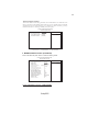
Using BIOS
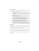
Advanced Chipset Features
These items define critical timing parameters of the motherboard. You should leave the
items on this page at their default values unless you are very familiar with the technical
specifications of your system hardware. If you change the values incorrectly, you may
introduce fatal errors or recurring instability into your system.
DRAM Clock/Drive Control [Press Enter]
CPU & PCI Bus Control [Press Enter]
System BIOS Cacheable [Enabled]
Video RAM Cacheable [Disabled]
Item Help
Menu Level
Phoenix-AwardBIOS CMOS Setup Utility
Advanced Chipset Features
F5:Previous Values F6:Fail-Safe Defaults F7:Optimized Defaults
: Move Enter: Select +/-/PU/PD:Value F10:Save ESC:Exit F1: General Help
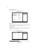
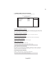
DRAM Clock/Drive Control
Scroll to this item and press <Enter> to view the following screen:
(Press Enter)
Item Help
Menu Level
Phoenix-AwardBIOS CMOS Setup Utility
DRAM Clock/Drive Control
F5:Previous Values F6:Fail-Safe Defaults F7:Optimized Defaults
: Move Enter: Select +/-/PU/PD:Value F10:Save ESC:Exit F1: General Help
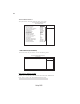
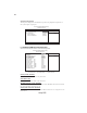
x
Current FSB/DRAM Frequency (100MHz/200MHz)
DRAM Clock
DRAM Timing
SDRAM CAS Latency [ DDR/DDR 2.5 / 4]
Bank Interleave Disabled
Precharge to Active (Trp) 4T
Active to Precharge (Tras) 07T
Active to CMD (Trcd) 4T
REF to ACT/REF (Trfc) 21T
ACT (0) to ACT(1) (TRRD) 3T
Read to Precharge (Trtp) [2T]
Write to Read CMD (Twtr) [1T/2T]
Write Recovery Time (Twr) [4T]
DRAM Command Rate [2T Command]
RDSAIT mode [Auto]
RDSAIT selection 03
This item displays current FSB/DRAM frequency.
Current FSB Frequency 100MHz
Current DRAM Frequency 200MHz
[By SPD]
x
x
x
x
x
x
x
[Auto By SPD]