
User Manual


33
Using BIOS
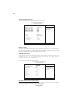
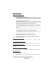
PCI Master 0 WS Write (Enabled)
This item determines whether the chipsets inserts a delay before any writes from the PCI
slots. If it is enabled, write requests to the PCI bus are executed immediately (with zero wait
states), if the PCI bus is ready to send data.
PCI Delay Transaction (Enabled)
This item is used to meet the latency of PCI cycles to and from the ISA bus.
VLink mode selection (By Auto)
This item controls the data transfer speed between the north and south bridge.
PCI Master 0 WS Write [Enabled]
PCI Delay Transaction [Enabled]
VLink mode selection [By Auto]
VLink 8X Support [Enabled]
DRDY_Timing [Default]
Item Help
Menu Level
F5:Previous Values F6:Fail-Safe Defaults F7:Optimized Defaults
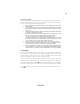
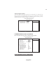
CPU & PCI Bus Control (Press Enter)
Scroll to this item and press <Enter> to view the following screen:
Phoenix-AwardBIOS CMOS Setup Utility
CPU & PCI Bus Control
: Move Enter: Select +/-/PU/PD:Value F10:Save ESC:Exit F1: General Help
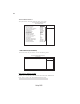
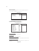
VLink 8X Support (Enabled)
Use this item to enable or disable VLink 8X support.
This item specifies the timing of data ready.
DRDY_Timing (Default)
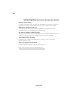
System BIOS Cacheable (Enabled)
This feature is only valid when the system BIOS is shadowed. It enables or disables the
caching of the system BIOS ROM at F0000h-FFFFFh via the L2 cache. This greatly
speeds up accesses to the system BIOS.
Video RAM Cacheable (Disabled)
Disable or enable this item to read cache data from RAM.
Press <Esc> to return to the Advanced Chipset Features page.
Press <Esc> to return to the main BIOS setting page.