
Datasheet


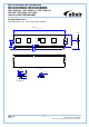

M2F1G64CBH4B5P/ M2F1G64CBH4B9P
M2F(X)2G64CB88B7N / M2F(X)2G64CB88BHN
M2F(X)4G64CB8HB5N / M2F(X)4G64CB8HB9N
1GB: 128M x 64 / 2GB: 256M x 64 / 4GB: 512M x 64
PC3-8500 / PC3-10600 / PC3-12800
Unbuffered DDR3 SDRAM DIMM
REV 1.0 21
05/2010
© NANYA TECHNOLOGY CORPORATION
NANYA reserves the right to change products and specifications without notice.
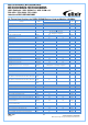
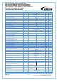
AC Timing Specifications for DDR3 SDRAM Devices Used on Module (1333MHz)
Parameter
Symbol
DDR3-1333
Units
Notes
Min.
Max.
Clock Timing
Minimum Clock Cycle Time (DLL off mode)
tCK (DLL_OFF)
8
-
ns
Average Clock Period
tCK(avg)
Refer to "Standard Speed Bins)
ps
Average high pulse width
tCH(avg)
0.47
0.53
tCK(avg)
Average low pulse width
tCL(avg)
0.47
0.53
tCK(avg)
Absolute Clock Period
tCK(abs)
Min.: tCK(avg)min + tJIT(per)min
Max.: tCK(avg)max + tJIT(per)max
ps
Absolute clock HIGH pulse width
tCH(abs)
0.43
-
tCK(avg)
Absolute clock LOW pulse width
tCL(abs)
0.43
-
tCK(avg)
Clock Period Jitter
JIT(per)
-80
80
ps
Clock Period Jitter during DLL locking period
JIT(per, lck)
-70
70
ps
Cycle to Cycle Period Jitter
tJIT(cc)
160
160
ps
Cycle to Cycle Period Jitter during DLL locking period
JIT(cc, lck)
140
140
ps
Duty Cycle Jitter
tJIT(duty)
-
-
ps
Cumulative error across 2 cycles
tERR(2per)
-118
118
ps
Cumulative error across 3 cycles
tERR(3per)
-140
140
ps
Cumulative error across 4 cycles
tERR(4per)
-155
155
ps
Cumulative error across 5 cycles
tERR(5per)
-168
168
ps
Cumulative error across 6 cycles
tERR(6per)
-177
177
ps
Cumulative error across 7 cycles
tERR(7per)
-186
186
ps
Cumulative error across 8 cycles
tERR(8per)
-193
193
ps
Cumulative error across 9 cycles
tERR(9per)
-200
200
ps
Cumulative error across 10 cycles
tERR(10per)
-205
205
ps
Cumulative error across 11 cycles
tERR(11per)
-210
210
ps
Cumulative error across 12 cycles
tERR(12per)
-215
215
ps
Cumulative error across n = 13, 14 . . . 49, 50 cycles
tERR(nper)
tERR(nper)min = (1 + 0.68ln(n)) * tJIT(per)min
tERR(nper)max = (1 + 0.68ln(n)) * tJIT(per)max
ps
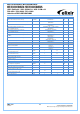
Data Timing
DQS, DQS# to DQ skew, per group, per access
tDQSQ
-
125
ps
DQ output hold time from DQS, DQS#
tQH
0.38
-
tCK(avg)
DQ low-impedance time from CK, CK#
tLZ(DQ)
-500
250
ps
DQ high impedance time from CK, CK#
tHZ(DQ)
-
250
ps
Data setup time to DQS, DQS# referenced to Vih(ac) / Vil(ac) levels
tDS(base)
AC175
-
ps
Data setup time to DQS, DQS# referenced to Vih(ac) / Vil(ac) levels
tDS(base)
AC150
30
ps
Data hold time from DQS, DQS# referenced to Vih(dc) / Vil(dc) levels
tDH(base)
DC100
65
ps
DQ and DM Input pulse width for each input
tDIPW
400
-
ps
Data Strobe Timing
DQS,DQS# differential READ Preamble
tRPRE
0.9
Note 19
tCK(avg)
DQS, DQS# differential READ Postamble
tRPST
0.3
Note 11
tCK(avg)
DQS, DQS# differential output high time
tQSH
0.4
-
tCK(avg)
DQS, DQS# differential output low time
tQSL
0.4
-
tCK(avg)
DQS, DQS# differential WRITE Preamble
tWPRE
0.9
-
tCK(avg)
DQS, DQS# differential WRITE Postamble
tWPST
0.3
-
tCK(avg)
DQS, DQS# rising edge output access time from rising CK, CK#
tDQSCK
-255
255
tCK(avg)
DQS and DQS# low-impedance time
(Referenced from RL - 1)
tLZ(DQS)
-500
250
tCK(avg)
DQS and DQS# high-impedance time
(Referenced from RL + BL/2)
tHZ(DQS)
-
250
tCK(avg)
DQS, DQS# differential input low pulse width
tDQSL
0.45
0.55
tCK(avg)
DQS, DQS# differential input high pulse width
tDQSH
0.45
0.55
tCK(avg)
DQS, DQS# rising edge to CK, CK# rising edge
tDQSS
-0.25
0.25
tCK(avg)
DQS, DQS# falling edge setup time to CK, CK# rising edge
tDSS
0.2
-
tCK(avg)
DQS, DQS# falling edge hold time from CK, CK# rising edge
tDSH
0.2
-
tCK(avg)