
Datasheet

M2U1G64DS8HB1G / M2U51264DS88B1G / M2U25664DSH4B1G
M2Y1G64DS8HB1G / M2Y51264DS88B1G / M2Y25664DSH4B1G (Green)
1GB, 512MB and 256MB
PC3200 and PC2700
Unbuffered DDR DIMM
REV 1.2 1
June 2, 2006
.
184 pin Unbuffered DDR DIMM
Based on DDR400/333 512M bit Die B device
Features
• 184 Dual In-Line Memory Module (DIMM)
• Unbuffered DDR DIMM based on 110nm 512M bit die B device
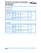
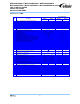
• Performance:
Speed Sort
PC2700
6K
PC3200
5T
DIMM Latency 2.5 3
Unit
f
CK
Clock Frequency 166 200 MHz
t
CK
Clock Cycle 6 5 ns
f
DQ
DQ Burst Frequency
333 400 MHz
• Intended for 200 and 166 MHz applications
• Inputs and outputs are SSTL-2 compatible
• V
DD
= V
DDQ
= 2.5V ± 0.2V (6K); V
DD
= V
DDQ
= 2.6V ± 0.1V (5T)
• SDRAMs have 4 internal banks for concurrent operation
• Differential clock inputs
• Data is read or written on both clock edges
• DRAM DLL aligns DQ and DQS transitions with clock transitions
• Address and control signals are fully synchronous to positive
clock edge
• Programmable Operation:
- DIMM Latency: 2, 2.5 (6K); 2.5, 3 (5T)
- Burst Type: Sequential or Interleave
- Burst Length: 2, 4, 8
- Operation: Burst Read and Write
• Auto Refresh (CBR) and Self Refresh Modes
• Automatic and controlled precharge commands
• 7.8 µs Max. Average Periodic Refresh Interval
• Serial Presence Detect EEPROM
• Gold contacts on module PCB
Description
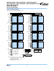
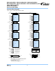
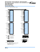
M2U1G64DS8HB1G and M2Y1G64DS8HB1G are unbuffered 200-Pin Double Data Rate (DDR) Synchronous DRAM Unbuffered Dual In-Line
Memory Module (UDIMM) and are organized as two ranks of 128Mbx64 high-speed memory array using sixteen 64Mx8 DDR SDRAMs TSOP
packages. M2U51264DS88B1G and M2Y51264DS88B1G are unbuffered 200-Pin DDR Synchronous DRAM UDIMM and are organized as a
single rank of 64Mbx64 high-speed memory array using eight 64Mx8 DDR SDRAMs TSOP packages. M2U25664DSH4B1G and
M2Y25664DSH4B1G are unbuffered 200-Pin DDR Synchronous DRAM UDIMM and are organized as a single rank of 32Mbx64 high-speed
memory array using four 32Mx16 DDR SDRAMs TSOP packages.
Depending on the speed grade, these DIMMs are intended for use in applications operating up to 200 MHz clock speeds and achieves
high-speed data transfer rates of up to 400 MHz. Prior to any access operation, the device latency and burst /length/operation type must be
programmed into the DIMM by address inputs and I/O inputs BA0 and BA1 using the mode register set cycle.
The DIMM uses a serial EEPROM and through the use of a standard IIC protocol the serial presence-detect implementation (SPD) can be
accessed. The first 128 bytes of the SPD data are programmed with the module characteristics as defined by JEDEC.