
Specifications


Chapter 2 – Hardware Resources
32 PL 3120/PL 3150/PL 3170 Power Line Smart Transceiver Data Boo
k
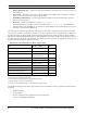
Stack Initialization and BIST 42.50 ms
SERVICE~ Pin Initialization 0.10 ms
State Initialization 0.13 ms
Off-Chip RAM Initialization 353.00 ms
Random Number Seed Calculation 5.00 ms
System RAM Setup 4.20 ms
Communication Port Initialization 0 ms
Checksum Initialization 12.50 ms
One-Second Timer Initialization 0.61 ms
Scheduler Initialization 0.74 ms
Total 418.78 ms
Use the following compiler directive to disable testing of off-chip RAM:
# pragma ram_test_off
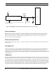
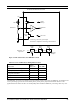
SERVICE~ Pin
The SERVICE~ pin alternates between input and open-drain output at a 76 Hz rate with a 50% duty cycle with a
10MHz input clock. At 6.5536MHz, the SERVICE~ pin alternates at a 50 Hz rate. When it is an output, it can sink 20
mA for use in driving a LED. When it is used exclusively as an input, it has an optional on-chip pull-up to bring the
input to an inactive-high state for use when the LED and pull-up resistor are not connected. Under control of the Neuron
firmware, this pin is used during configuration, installation, and maintenance of the device containing the PL Smart
Transceiver. The firmware flashes the LED at a 1/2 Hz rate when the PL Smart Transceiver has not been configured
with network address information. Grounding the SERVICE~ pin causes the PL Smart Transceiver to transmit a
network management message containing its unique 48-bit Neuron ID and the application’s program ID on the network.
This information can then be used by a network tool to install and configure the device. A typical circuit for the
SERVICE~ pin LED and push-button is shown in Figure 2.11. During reset the SERVICE~ pin state is indeterminate.
The default state of the SERVICE~ pin pull-up is enabled.