
Specifications

Chapter 3 – Input/Output Interfaces
38 PL 3120/PL 3150/PL 3170 Power Line Smart Transceiver Data Boo
k
Introduction
The PL 3120, PL 3150, and PL 3170 Power Line Smart Transceivers connect to application-specific external hardware
via 12 pins, named IO0-IO11. These pins can be configured in numerous ways to provide flexible input and output
functions with minimal external circuitry. The programming model (Neuron C language) allows the programmer to
declare one or more pins as I/O objects. An I/O object provides programmable access to an I/O driver for a specified on-
chip I/O hardware configuration and a specified input or output waveform definition. With the exception of the SCI
(UART) model, the user’s program can then refer to these objects in io_in and io_out() system calls to perform
the actual input/output function during execution of the program. Certain events are associated with changes in input
values. The task scheduler can thus execute associated application code when these changes occur.
There are many different I/O objects available for use with the PL Smart Transceivers. Most I/O Objects are available in
the PL 3150, PL 3120, and PL 3170 Smart Transceiver system images by default. If an object that is not included in the
default system image is required by an application, the development tool will link the appropriate object(s) into available
memory space. For PL 3120 and PL 3170 Smart Transceiver designs, this means that internal EEPROM space must be
used for the additional object. For PL 3150 Smart Transceiver designs, the object will be added to an external flash or
ROM region beyond the 16KB space reserved for the system image.
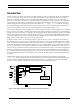
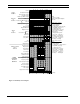
PL Smart Transceivers have two 16-bit timer/counters on-chip (see Figure 2.7 and 3.1). The input to timer/counter 1,
also called the multiplexed timer/counter, is selectable among pins IO4 – IO7, via a programmable multiplexer (MUX)
and its output can be connected to pin IO0. The input to timer/counter 2, also called the dedicated timer/counter, can be
connected to pin IO4 and its output to pin IO1. The timer/counters are implemented as a 16-bit load register writable by
the CPU, a 16-bit counter, and a 16-bit latch readable by the CPU. The load register and latch are accessed a byte at a
time. No I/O pins are dedicated to timer/counter functions. If, for example, timer/counter 1 is used for input signals only,
then IO0 is available for other input or output functions. Timer/counter clock and enable inputs can be from external
pins, or from scaled clocks derived from the system clock; the clock rates of the two timer/counters are independent of
each other. External clock actions occur optionally on the rising edge, the falling edge, or both rising and falling edges
of the input.
Multiple timer/counter input objects can be declared on different pins within a single application. By calling the
io_select() function, the application can use the first timer/counter to implement up to four different input objects.
If a timer/counter is configured to implement one of the output objects, or is configured as a quadrature input object,
then it can not be reassigned to another timer/counter object in the same application program.
System Clock
Divide Chain
Timer/Counter 1
Timer/Counter 2
IO10
IO9
IO8
IO0
IO1
IO2
IO3
IO4
IO5
IO6
IO7
mux
20 mA Sink Capability
Programmable Pull-Up Capability
IO11
Figure 3.1 PL Smart Transceiver Timer/Counter External Connections