
User manual

AOAA Kit - User’s Guide
Page 25
Copyright 2012 © Embedded Artists AB
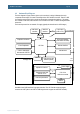
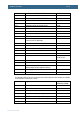
4.6 Hardware Block Diagram
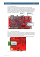
The block diagram in Figure 18 below gives a quick overview of a design. It illustrates the major
components in the design. The center of the design is the LPC1769 MCU from NXP. There is a USB
Host interface to the Android device as well as several other communication interfaces. The design
also contains a CAN node, built around the LPC11C24 MCU from NXP. It contains an integrated CAN
transceiver.
The board is powered from an external +5V supply (typically the Android device’s USB charger).
Figure 18 – The AOAA Board Block Diagram
Both MCUs have SWD interfaces for program download. The LPC1769 also supports program
download via UART (there is an UART-to-USB bridge that also support automatic ISP activation).
LPC1769
RF-module interface
(NXP/Jennic and XBee)
Power input
(USB or +5V)
USB Host
interface
USB Device
interface
IO and Peripherals
CAN interface
Ethernet interface
CAN
network
Temperature and Light
sensors on I
2
C
CAN node side
I
2
C
+5V
LPC11C24
CAN microcontroller
SWD I/F
SWD I/F
LEDs and push button
Expansion connector
Expansion connectors
Select
+3.3V
+5V to CAN network
Power supply
+3.3V
UART-to-USB bridge
with automatic ISP func.
Prototype area
uSD memory card
interface (via SPI)