
User manual

AOAA Kit - User’s Guide
Page 27
Copyright 2012 © Embedded Artists AB
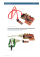
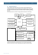
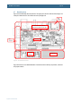
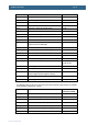
Figure 20 – The AOAA Board Overview, part 2
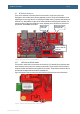
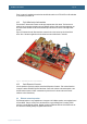
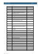
4.8 Usage of CPU Pins
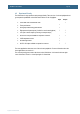
The table below lists how the LPC1769 pins are used in the design and which ones are available on
the expansion connector, J12.
LPC1769 pin
Usage
Expansion
connector (J12)
P0_0, P0_1
CAN interface
P0_2, P0_3
UART#0 connected to UART-to-USB bridge
P0_4
Not used, free for expansion
Pin 1
P0_5
Not used, free for expansion
Pin 3
P0_6 – P0_9
SPI#1 connected to uSD interface and serial expansion
connector.
Pin 5 (P0_6),
Pin 7 (P0_7),
Pin 9 (P0_8),
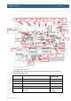
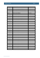
JP3
J12, expansion
connector
SW5, push-
button
LED12,
RGB-LED
J1, SWD i/f for
LPC1769
J4, Ethernet
connector
J2,USB Device
connector
JP1/JP2
up (pos1-2)= USB Device
down (pos2-3)=USB Host
J2,USB Host
connector
J14,USB-B
power input
J15,power
input (alt +5V)
RF2,XBee
socket
RF1,JN5148
pads on
bottom side
J22,uSD
connector
J13, 8
prot. I/O
J7, serial exp.
connector
J21, SWD i/f
for LPC11C24
SW4, Reset
J16, UART-
to-USB i/f
R93,
trim.pot.
Top-to-bottom:
LED6 / SW2
LED7 / SW3
J11, 4 OD
I/O
JP4
J8