
User manual

AOAA Kit - User’s Guide
Page 32
Copyright 2012 © Embedded Artists AB
o All pins of the JN5148 modules are not connected. Only the ones needed to get a
UART communication channel with the board.
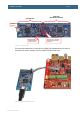
Digi’s XBee family of radio modules
The interface to this module is located on the top/component side of the board. There are two
1x10 pos, 2mm pitch sockets for inserting the XBee module.
o Only the pins needed for UART communication have been connected to the
LPC1769. There is an option to use three data flow modem signals also (RTC, CTS
and DTR) via JP3.
All pins of the XBee module is accessible connectors J9 and J10 that are located
just beside the XBee modules.
o Three LEDs have been added that can signal different states of the operation.
Note that only one module at a time can be connected.
There are different (application) versions of the radio modules which gives the flexibility to create
different types of radio node networks. There are also several radio modules that build upon the same
form factor as the XBee module.
4.9.6 Page 7
There is a uSD memory card interface connector, J22. The memory card can be accessed via the SPI
peripheral, which is 1-bit serial. The higher-throughput 4-bit parallel interface that also exists on these
memory cards cannot be used. There is a voltage switch implemented by a p-channel mosfet (Q9)
controlled by signal P0.18. LED14 is on when the uSD interface is powered. LED15 is on when a uSD
memory card is inserted into the (J22) connector and this can also be detected via signal P0.19. A low
signals indicated that a uSD memory card is inserted.
4.9.7 Page 8
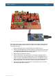
There are some basic peripherals in the design for direct prototyping/experimenting with the AOAA
application. There are also general expansion interfaces for external circuits.
As basic peripherals there are:
Two RGB-LEDs (LED6 and LED7) are connected to PWM outputs of the LPC1769.
Two push buttons are connected to interrupt inputs of the LPC1769.
A trimming potentiometer (R93) is connected to analog input #5 of the LPC1769.
For general expansion there are:
Eight protected inputs/outputs. The I/Os are protected with series resistors, filtering capacitors
and clamping diodes.
Four open drain outputs. These outputs can be used to drive relays and opto-couplers for
controlling larger loads. There are clamping diodes that can be connected to the external
power supply (pin 5 of J11), typically a 5, 12, or 24 supply. Check the BSH111 datasheets for
details about switching capabilities.
Expansion connector (J12) that contains all available LPC1769 pins – ‘available’ in the sense
of not used for other purposes. These LPC1769 pins are directly connected to the connector
and there is no protection. Pins that have dedicated use on the AOA board are not included in
the connector. Note that some of the pins on the expansion connector can be used by other
functionalities on the board but the user can select to not make use of these functions. For
example, the SPI interface is used by the uSD memory card interface and the PWM signals
control the RGB-LEDs. It is still however possible to use the SPI and PWM interface for
external expansion via J12.