
User manual

AOAA Kit - User’s Guide
Page 33
Copyright 2012 © Embedded Artists AB
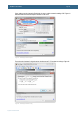
4.9.8 Page 9
The board is normally powered via J14, a USB-B connector where the Android device’s charger is
connected. Alternatively an external +5VDC, 1A supply can be connected via J15, a 2.1mm power jack
input. The power supply is very simple, an LDO to create the +3.3V from the +5V input.
There is a UART-to-USB bridge based on the FT232RL chip from FTDI. It is connected to UART#0 on
the LPC1769. When inserting both jumpers in JP4 (pin 1-2 and 3-4) the automatic ISP activation
functionality is enabled. The modem signals RTS and DTS modem can control reset and pulling pin
P2.10 low, hence enabling In-System Programming (ISP) mode. It is an internal boot loader mode for
downloading code into the LPC1769 over the UART. The PC application FlashMagic
(http://www.flashmagictool.com) can be used for this.
Voltage supervisor, U12, generate a proper reset to the system. Reset-LED LED11 is on whenever
reset is active. There is also a Reset push button, SW4 for generating manual resets.
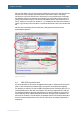
4.9.9 Page 10
The last schematic page contains the LPC11C24 CAN node. It is a separate part f the design on the
sense that it is physically separated on the pcb and the only connection to the LPC1769 is via the on-
board CAN network.
The LPC11C24 CAN node can be broken off from the AOA board. The node can still be connected to
a CAN network via a DSUB9 (J18) or RJ45 (J17) connector. Note that these connectors are
overlapping on the board so only one can be used at a time. These connectors are not mounted but
can easily be soldered, if needed. The connectors follow standard CAN pinning.
The center of the CAN node is the LPC11C24 from NXP. It is a MCU based on the ARM Cortex-M0
core and has integrated CAN transceiver in the package. The external crystal is 12MHz, which is the
recommended value to get standard CAN timing.
The CAN node is powered via the +5V supply that is part of the CAN network. LDO U13 generates the
needed local +3.3V supply.
There are two sensors connected to the I
2
C channel:
The ISL29003 ambient light sensor from Intersil. The I2C address to the ISL29003 is 0x44
(1.0.0.0.1.0.0.rw). Details about the ISL29003 operation can be found in the datasheet.
The LM75B temperature sensor is from NXP. The I2C address to the LM75B is 0x48
(1.0.0.1.0.0.0.rw). Details about the LM75B operation can be found in the datasheet.
There is an RGB-LED, LED12 as well as a single LED, LED13. There is also a push button, SW5,
connected to pin PIO1_4. This is the wakeup input to the LPC11C24, which can be useful if
experimenting with the power down modes of the MCU.
J21 is the SWD interface for LPC11C24, i.e., debug interface. It is the new and smaller footprint
standard ARM debug connector. It has 2x5 pins in 50 mil pitch.
All pins of the LPC11C24 are available on the edge expansion connectors, J19 and J20. These are
2.54mm/100 mil pitch connectors placed 17.78 mm / 700 mil apart.