
User manual


LCD Board - User’s Guide
Page 9
Copyright 2012 © Embedded Artists AB
4 LCD Board Design
This chapter describes the hardware design of the LCD Board. The schematic can be downloaded
from the support page after registering the product serial key (that comes with purchase of the LCD
Board). It can be good to have the schematic side by side when reading this chapter.
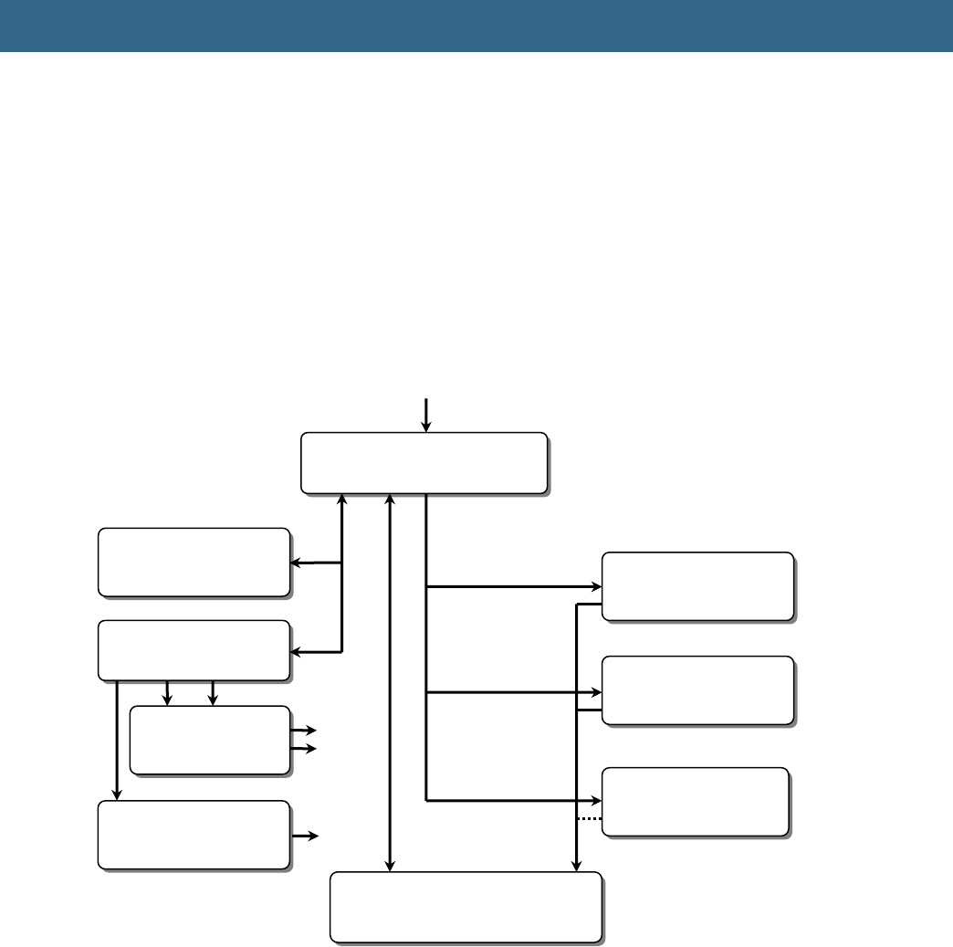
4.1 Block Diagram
The block diagram in Figure 2 below gives a quick overview of a design. It illustrates the major
components in the design.
Figure 2 – The LCD Board Block Diagram
4.2 Schematic Walkthrough
4.2.1 Page 2
J1 is the interface connector to the board. It carries the parallel RGB pixel data as well as control
signals. SPI and I2C serial channels are also present.
The data signals are connected to that TFT5:6:5 and TFT4:4:4 modes of the LPC on-chip LCD
controllers are supported.
All high-speed signals have 100 ohm series resistors in order to minimize signal reflections on the
board.
There is a 40MHz oscillator that can generate a pixel clock to the LPC LCD controller. This shall
currently not be used since 40MHz will create a higher memory bus load than most designs can
handle. The frequency will be changed to 33.333MHz in later revisions of the boards. The oscillator is
normally only mounted on 7 inch LCD Board.
50-pos (2x25) shrouded
IDC connector
I2C-GPIO (PCA9532)
Resistive touch screen controller
(TSC2046) with SPI interface
I2C-E2PROM with
configuration data
Voltage
sequence control
4.3 inch (480x272
pixels) TFT LCD
7.0 inch (800x480
pixels) TFT LCD
Parallel RGB interface (16/12 bit)
+ I2C/SPI bus
I2C
More LCDs to be
supported…
LCD_3.3V
LCD_5.0V
SPI
Parallel RGB pixel data
Backlight
voltage generation
LCD_BL
20-40mA