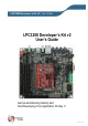
LPC3250 Developer’s Kit v2 - User’s Guide Copyright 2013 © Embedded Artists AB LPC3250 Developer’s Kit v2 User’s Guide Get Up-and-Running Quickly and Start Developing Your Application On Day 1! EA2-USG-1204 Rev A
LPC3250 Developer’s Kit v2 - User’s Guide Page 2 Embedded Artists AB Davidshallsgatan 16 211 45 Malmö Sweden info@EmbeddedArtists.com http://www.EmbeddedArtists.com Copyright 2013 © Embedded Artists AB. All rights reserved.
LPC3250 Developer’s Kit v2 - User’s Guide Page 3 Table of Contents 1 Document Revision History 6 2 Introduction 7 2.1 Features 7 2.2 ESD Precaution 8 2.3 General Handling Care 9 2.4 LPC3250 Core Voltage Precaution 9 2.5 CE Assessment 9 2.6 Other Products from Embedded Artists 9 2.6.1 Design and Production Services 2.6.2 OEM / Education / QuickStart Boards and Kits 3 LPC3250 OEM Board Design 3.1 LPC3250 OEM Board Schematics 10 11 11 3.1.1 Schematic Page 2: Crystals 11 3.1.
LPC3250 Developer’s Kit v2 - User’s Guide Page 4 4.14 SP8: NXP/Jennic RF Module Interface 27 4.15 SP9: UART Multiplexing 28 4.16 SP9: RS232 Interface 29 4.17 SP9: RS422/485 Interface 30 4.18 SP10: CAN 31 4.19 SP10: IrDA 32 4.20 SP11: USB Channel 1 33 4.20.1 USB Channel 1 as USB Host 34 4.20.2 USB Channel 1 as USB Device 34 4.20.3 USB Channel 1 as USB OTG 34 4.21 SP12: USB Channel 2 4.21.1 USB Channel 2 as USB Host 36 4.21.2 USB Channel 2 as USB Device 36 4.21.
LPC3250 Developer’s Kit v2 - User’s Guide Page 5 7.1 Powering 64 7.2 Contact with OEM Board MCU 65 7.
LPC3250 Developer’s Kit v2 - User’s Guide Page 6 1 Document Revision History Revision Date Description A 2012-06-18 First official revision of document for the OEM Base Board PB1 2012-10-16 Clarified I2S jumper positions in Figure 25. PB2 2013-06-05 Correction about which connector to use for USB Device on USB2.
LPC3250 Developer’s Kit v2 - User’s Guide Page 7 2 Introduction Thank you for buying Embedded Artists’ LPC3250 Developer’s Kit based on NXP’s ARM926EJ-S LPC3250 microcontroller. This document is a User’s Guide that describes the LPC3250 OEM Board and the OEM Base Board hardware design, which together form the LPC3250 Developer’s Kit. Note that there is a previous version of the LPC3250 Developer’s Kit that was based on the QVGA Base Board.
LPC3250 Developer’s Kit v2 - User’s Guide USB2: Device or Host interface & connector Provision for NXP JN5148 RF module (former Jennic) interface (RF module not included) Full modem RS232 RS422/485 interface & connector Provision for IrDA transceiver interface (transceiver not mounted) I2S audio codec (mic in, line in, line out, headphone out) JTAG connector Trace/ETM connector (not mounted) Power 2.
LPC3250 Developer’s Kit v2 - User’s Guide 2.3 Page 9 General Handling Care Handle the LPC3250 OEM Board and OEM Base Board with care. The boards are not mounted in a protective case/box and are not designed for rough physical handling. Connectors can wear out after excessive use. The OEM Base Board is designed for prototyping use, and not for integration into an end-product. For boards with LCD, do not exercise excessive pressure on the LCD glass area. That will damage the display.
LPC3250 Developer’s Kit v2 - User’s Guide Page 10 communication interfaces, specific analog or digital I/O, and power supplies. Embedded Artists has a broad, and long, experience in designing industrial electronics in general and with NXP’s LPC1000/2000/3000/4000 microcontroller families in specific. Our competence also includes wireless and wired communication for embedded systems. For example IEEE802.11b/g (WLAN), Bluetooth™, ZigBee™, ISM RF, Ethernet, CAN, RS485, and Fieldbuses. 2.6.
LPC3250 Developer’s Kit v2 - User’s Guide Page 11 3 LPC3250 OEM Board Design Please read the LPC3250 OEM Board datasheet and associated schematic for information about the board. Some additional information about the LPC3250 OEM Board is presented below. 3.1 LPC3250 OEM Board Schematics 3.1.1 Schematic Page 2: Crystals The microprocessor crystal frequency is 13.0000 MHz, which is the recommended frequency from NXP. An internal PLL can create many other frequencies from this, like 208 MHz and 266 MHz.
LPC3250 Developer’s Kit v2 - User’s Guide Page 12 There are 2.2 kohm pull-up resistors (pull-ups are always needed on I2C busses) on the board on both I2C channels. 3.1.6 Schematic Page 3: 1.2V and 1.8V Fixed Voltages The LPC3250 requires three fixed voltages; 1.2V for the core, 1.8V for the memory interface and 3.153.3V for the rest of the i/o interfaces. The 1.2V and 1.8V voltages are generated by two LM3671MF step-down switching regulators from National Semiconductor.
LPC3250 Developer’s Kit v2 - User’s Guide 3.1.11 Page 13 Schematic Page 4: NAND Flash A 1 Gbit (128 MByte) NAND flash is used (K9F1G08 from Samsung). The chip is powered by 3.3V and has 8-bit databus width. The NAND flash builds on a single-level cell (SLC) technology and has a page size of 2112 bytes (2,048 + 64 bytes). Note that the chip is not directly accessible via the memory bus. Instead, all accesses must be done via the on-chip NAND flash controller of the LPC3250.
LPC3250 Developer’s Kit v2 - User’s Guide Static memory #2 CS2 Page 14 0xE200 0000 – 0xE2FF FFFF Available for external use. OEM Base Board can connect a parallel NOR flash to this chip select. Static memory #3 CS3 0xE300 0000 – 0xE3FF FFFF Available for external use. OEM Base Board can connect a 16-bit parallel register to this chip select. Dynamic memory #0 DYCS0 Dynamic memory #1 DYCS1 0x8000 0000 – 0x9FFF FFFF SDRAM (512 MBit = 64 MByte in size) Cannot be accessed on external memory bus.
LPC3250 Developer’s Kit v2 - User’s Guide Page 15 4 OEM Base Board Design This chapter contains information about the peripherals and general design of the OEM Base Board and how to set the different jumpers on the board. The schematic can be downloaded in pdf format from the support page, and is recommended to have printed out while reading this chapter. Section naming begins with SPx, which is short for Schematic Page x. The picture below gives an overview of the OEM Base Board design.
LPC3250 Developer’s Kit v2 - User’s Guide 4.1 Page 16 Modifications to OEM Base Board The OEM Base Board has been designed to be flexible. Most options can be controlled via jumpers but some options might need soldering. Note that modifications to the board are done at own risk and void all warranties. 4.2 SP2: OEM Board Connector The LPC3250 OEM board connector is a standard DDR2 SO-DIMM socket with 200 positions and 0.6mm pitch. The JEDEC standard for this form factor is called MO-224. It has 1.
LPC3250 Developer’s Kit v2 - User’s Guide Page 17 Expansion Connectors left to right: J4, J3, J5 Figure 3 – Expansion Connectors J3, J4, J5 4.5 SP4: External Memory Bus This part of the OEM Base Board demonstrates how the external memory bus can be used for expansion of custom circuits. Two different devices are connected to the memory bus; a 16-bit parallel NOR flash and a 16-bit register. In order to be universal between 16- and 32-bit databus width OEM Boards, only the lower 16 bits are connected.
LPC3250 Developer’s Kit v2 - User’s Guide Page 18 signal BCS3. This means that the 16-bit register is accessible in memory region: 0xE300 0000 0xE3FF FFFF. No jumper in JP2 is needed when working with the LPC3250 OEM Board. SJ12 shall be in default position (pad 1-2 shorted) to let BCS2 control chip select of the 16-bit register. SJ1 controls the output enable of the register. By default it is grounded (pad 1-2 is shorted) and hence the register drives the LEDs and expansion connector, J6.
LPC3250 Developer’s Kit v2 - User’s Guide Page 19 When working with the LPC3250 OEM Board, J7 is typically used. If an older and big footprint JTAG debug pod is used, J8 can alternatively be used. JP3, J9 and J10 are not used when working with LPC3250 OEM boards. JP4 shall be open (no jumper inserted) for enabling the JTAG interface of the LPC3250 OEM board. Also note that the LPC3250 has a JTAG interface. Not the newer SWD interface.
LPC3250 Developer’s Kit v2 - User’s Guide 4.7 Page 20 SP6: Ethernet Interface The board has an Ethernet interface, J11, which is a RJ45 connector with integrated magnetics. There is also provision on the board for connecting a PoE interface. All signals can be accessed via expansion pads, J12. Five 0 ohm resistors have to be removed in that case for isolating J11 from the new connector (this is because J11 is not capable of handling a PoE interface so a new RJ45 connector must added).
LPC3250 Developer’s Kit v2 - User’s Guide 4.8 Page 21 SP6: SD/MMC Memory Card Interface The board has a SD/MMC memory card interface, J13. Supply voltage to the external memory card is controlled via Q1. The Card Detection (CD) and Write Protect (WP) signals are connected to the I2C port expander on schematic page 7. There is also visual indication of supply voltage and the CD and WP signals via LEDs, see picture below where to find the LEDs on the board.
LPC3250 Developer’s Kit v2 - User’s Guide 4.9 Page 22 SP6: VBAT/ALARM Handling The board can power the VBAT input supply (to the OEM board) from two different sources: The +3.3V power supply, via D1 (when board is normally powered). A 3V Lithium CR1025 size coin battery, via D2. Note that battery is not included. See the LPC3250 datasheet for details about VBAT voltage range. The ALARM signal control LED21. It is the LPC3250 signal ONSW that is connected to this signal.
LPC3250 Developer’s Kit v2 - User’s Guide Page 23 4.10 SP7: I2C Peripherals There are several I2C peripherals on the board. See picture below for locating the different components on the board. The I2C addresses for the individual components are given in the schematic. Configuration E2PROM, 64kbit. This chip contains version information about the OEM Base Board. LM75 Temperature sensor. 3-axis Accelerometer (MMA7455). Note that the two interrupt outputs are not connected but available on JP5.
LPC3250 Developer’s Kit v2 - User’s Guide Page 24 4.11 SP8: Analog Input The board contains a trimming potentiometer (R94) for manually generating an adjustable voltage (between GND and VREF). See picture below where to locate the trimming potentiometer on the board. The table list which pin the adjustable voltage is connected to.
LPC3250 Developer’s Kit v2 - User’s Guide Page 25 4.12 SP8: Digital IO There is a push-button (SW6) that is connected to a signal that enable the service mode after reset on the OEM Board. For the LPC3250 this is pin GPI_01. If this pin is sampled low after reset, the uart service mode for the LPC3250 is entered (allowing program code download to internal SRAM via UART #5). LED30 is positioned above SW6 and will light when SW6 is pressed.
LPC3250 Developer’s Kit v2 - User’s Guide Serial Expansion Connector J15 Figure 12 – Serial Expansion Connector Signals LPC3250 GPIO29_SPI-CLK SPI1_CLK GPIO31_SPI-MISO SPI1_DATIN GPIO32_SPI-MOSI SPI1_DATIO GPIO69 P2.
LPC3250 Developer’s Kit v2 - User’s Guide Page 27 4.14 SP8: NXP/Jennic RF Module Interface There are pads on the backside of the OEM Base Board for soldering a JN5148 NXP (former Jennic) RF module. These pads are opposite of the SD/MMC memory card interface connector. There is also provision on the board for programming the RF module. This is done via 6-pos pin list (J31) where a FTDI programming cable is connected (TTL to USB Serial Converter cable, TTL-232R-3V3, see for example Digikey: 768-1015-ND).
LPC3250 Developer’s Kit v2 - User’s Guide Page 28 4.15 SP9: UART Multiplexing UART channels from four sources are multiplexed into one UART channel, which is connected to the OEM Board: Serial Expansion Connector / RF module. Note that if the RF module is soldered to the board, then UART channel on the Serial Expansion Connector is occupied.
LPC3250 Developer’s Kit v2 - User’s Guide Page 29 4.16 SP9: RS232 Interface There is a RS232 interface with all modem signals on the board. The RS232 interface is available on a 9-pos male DSUB. The OEM Base Board is a DTE (Data Terminal Equipment). An external device can be a DCE (Data Communications Equipment). For connecting DTE-to-DCE a straight-thru cable shall be used. An external device can also be a DTE. For connecting DTE-to-DTE a null-modem cable shall be used (also called a crossover cable).
LPC3250 Developer’s Kit v2 - User’s Guide Page 30 4.17 SP9: RS422/485 Interface There is a RS422/485 interface on the board. RS422 has individual transmit and receive pairs, while RS485 share the same signal pair (and is hence half-duplex). By inserting both jumpers in JP9, the two signal pairs are connected and a RS485 interface is created. By removing the jumpers in JP9 a RS422 interface is created. Via JP10 it is also possible to add termination resistors, if needed.
LPC3250 Developer’s Kit v2 - User’s Guide Page 31 4.18 SP10: CAN The CAN interface is not supported since there is no on-chip CAN peripheral on the LPC3250. For reference, the information about the interface is described below. There is one CAN interface mounted on the board. The board is also prepared for a second CAN interface, if needed. Via JP16 it is also possible to add termination resistors, if needed. The interface has on-board ESD protection. See picture below for locating relevant components.
LPC3250 Developer’s Kit v2 - User’s Guide Page 32 4.19 SP10: IrDA The board is prepared for an IrDA interface, but the IrDA transceiver (TFBS4652) is not mounted. To enable the IrDA interface, mount U18 (TFBS4652) and adjust SJ2 and SJ3 (connect 2-3 pads). See picture below for locating relevant components. The table below lists signal connections.
LPC3250 Developer’s Kit v2 - User’s Guide Page 33 4.20 SP11: USB Channel 1 The USB1 interface is not supported since there is one on-chip USB interface on the LPC3250 and this is connected to the USB2 interface on the OEM base board. For reference, the information about the interface is described below. The interface cannot be used. The USB1 interface offers a USB Host or USB OTG interface. Only one of these interfaces can be used at a time, i.e., both cannot be used simultaneously.
LPC3250 Developer’s Kit v2 - User’s Guide GPIO42 GPO_14. Not used for USB1 interface GPIO51 SPI2_DATIN. Not used for USB1 interface GPIO52 GPIO_04. Not used for USB1 interface GPIO53 SPI2_CLK. Not used for USB1 interface GPIO46 P0.6 normally not connected. Not used for USB1 interface GPIO43 GPI_03 normally not connected. Not used for USB1 interface 4.20.1 Page 34 USB Channel 1 as USB Host When USB channel #1 is used as USB Host, 15Kohm pull-down resistors are needed on the USB data signals.
LPC3250 Developer’s Kit v2 - User’s Guide Page 35 4.21 SP12: USB Channel 2 This section describes the second USB interface on the board. This is the interface that the USB interface on the LPC3250 is connected to. This interface has a USB Host connector (USB-A), a USB OTG (USB mini-B) and a USB Device connector (USB-B). One of these interfaces can be used at a time, i.e., both cannot be used simultaneously. The software on the LPC3250 OEM Board is also different between the interfaces.
LPC3250 Developer’s Kit v2 - User’s Guide Page 36 GPIO26 USB-VBUS-CTRL from USB OTG transceiver on LPC3250 OEM board GPIO55 GPI_02 GPIO66 USB-ID to USB OTG transceiver on LPC3250 OEM board 4.21.1 USB Channel 2 as USB Host When USB channel #2 is used as USB Host, JP17/JP18/JP19 shall all be set in position 2-3. J22 is the connector to use when USB Host is used. In order to provide +5V to the external USB device connected to this connector (J20), channel B of U20 must be enabled.
LPC3250 Developer’s Kit v2 - User’s Guide Page 37 4.22 SP13: UART-to-USB Bridge There is a UART-to-USB bridge on the board. This is to simplify connection to a PC because serial ports are not so common any more, especially not on laptops. The USB port also offers the possibility to power the board. It is UART#5 that is connected to the USB channel. This UART is commonly used as the console channel for applications. Printf() output is for example typically directed to this UART channel.
LPC3250 Developer’s Kit v2 - User’s Guide Page 38 4.23 SP13: Power Supply The power supply on the board is straight forward. There are three powering sources: 1. +5V DC via 2.1mm power jack (J24). Center pin positive. There is also an alternative connector (J23) for this powering option. 2. USB powering via the USB-to-UART Bridge connector (J25). 3. +5V DC power form the PoE (Power-over-Ethernet) connector (J12). In all cases, a stable +5V DC voltage powers the board.
LPC3250 Developer’s Kit v2 - User’s Guide Page 39 4.24 SP14: LCD Expansion Interface The board contains a buffered LCD expansion interface via a 50 pos IDC connector. The expansion interface also includes UART (see UART multiplexing), I2C and SPI interfaces. These additional interfaces are for identifying external displays (via configuration I2C-E2PROM) as well as touch screen controllers. An external LCD pixel clock can also be supplied via the expansion connector.
LPC3250 Developer’s Kit v2 - User’s Guide GPIO70 GPIO_00 GPIO42 GPO_14 Page 40 4.25 SP15: I2S Audio Codec The board contains an I2S audio codec based on UDA1380 from NXP. The codec is controlled via I2C and audio data is transferred over the I2S bus. The OEM Base Board supports different OEM Boards and the I2S signals can be located at two different groups of signals from the OEM Board. Jumper JP22-JP27 selects which group of signals to connect to the I2S interface of the UDA1380.
LPC3250 Developer’s Kit v2 - User’s Guide GPIO59 P0.0 / I2S1RX_CLK GPIO60 P0.
LPC3250 Developer’s Kit v2 - User’s Guide Page 42 4.26 Default Jumpers Positions Figure 25 illustrates the default jumper positions as mounted when the board is delivered from Embedded Artists. Default jumpers are marked with red color. Change JP22, JP23, JP24, JP25, JP26, JP27, JP28 to pos 2-3 Change JP34 to pos 2-3 Figure 25 – OEM Base Board Default Jumper Positions Note that the default position for the six I2S jumpers is not what is needed for the LPC3250 OEM board.
LPC3250 Developer’s Kit v2 - User’s Guide Page 43 4.27 Usage of CPU Pins Almost all pins of the LPC3250 are directly available on the expansion connectors. Only in a few cases are pins used for dedicated functionality like Ethernet interface and chip select signals. Such pins are not available on the expansion connector. The table below lists all pins and their possible restrictions.
LPC3250 Developer’s Kit v2 - User’s Guide Page 44 GPIO23 HICORE / LCDVD17 LCD databit 17 GPIO24 U1_TX Connects to UART multiplexing (TxD); further to LCD expansion connector, serial expansion connector, RF module, RS232 and RS422/485. GPIO25 U1_RX Connects to UART multiplexing (RxD); further to LCD expansion connector, serial expansion connector, RF module, RS232 and RS422/485. GPIO26 USB_VBUS_CTRL Connects to USB2 VBUS power enable. GPIO27 GPO_17 Connects to USB2-up LED (active low).
LPC3250 Developer’s Kit v2 - User’s Guide Page 45 MCIDAT1 MCIDAT1 Connects to MCIDAT1 on SD/MMC connector MCIDAT2 MCIDAT2 Connects to MCIDAT2 on SD/MMC connector MCIDAT3 MCIDAT3 Connects to MCIDAT3 on SD/MMC connector GPIO41 GPIO_05 No special usage on OEM Base Board, but is used for SPI_SSEL on the boot serial flash on the LPC3250 OEM board GPIO42 GPO_14 Connects to LCD expansion connector (backlight control). Connects to USB1-up LED (active low). Connects to serial expansion connector.
LPC3250 Developer’s Kit v2 - User’s Guide Page 46 GPIO60 P0.1 / I2SRX_WS Can be connected to I2S audio codec BCKI (I2SRX-WS) GPIO61 GPI_00 / I2SRX_SDA Can be connected to I2S audio codec BCKI (I2SRX-DATA) GPIO62 I2C2_SDA No special usage on OEM Base Board. GPIO63 I2C2_SCL No special usage on OEM Base Board. GPIO64 GPI_04 No special usage on OEM Base Board. GPIO65 GPI_06 No special usage on OEM Base Board.
LPC3250 Developer’s Kit v2 - User’s Guide Page 47 GPIO93 U3_DSR / U2_RX Can be connected to RS232 interface GPIO94 GPI_05 / U3_DCD Can be connected to RS232 interface GPIO95 U3_CTS / U2_CTS Can be connected to RS232 interface GPIO96 U3_RX Can be connected to RS232 interface GPIO97 U3_TX Can be connected to RS232 interface BD0-BD15 EMC_D0-EMC_D15 Connects to parallel NOR flash and 16-bit register. BA0-BA23 EMC_A0-EMC_A23 The address bus, buffered signals from OEM Board.
LPC3250 Developer’s Kit v2 - User’s Guide Page 48 5 Getting Started This chapter contains information about how to get acquainted with the LPC3250 Developer’s Kit. Please read this section first before you start using the board - it will be well spent time! 5.1 Powering The board can normally be powered from a PC/laptop via the included USB cable (mini-B to A cable). This is done via the USB-to-UART connector and will work in most cases.
LPC3250 Developer’s Kit v2 - User’s Guide Page 49 A USB driver must be installed on the PC/laptop in order for the virtual COM port to be created. See FTDI’s installation guides for details how to install the driver for different operating systems: http://www.ftdichip.com/Support/Documents/InstallGuides.htm 5.3 Building Sample Applications A bundle with sample applications is available at Embedded Artists’ support site.
LPC3250 Developer’s Kit v2 - User’s Guide 5.3.1 Page 50 Compile Using CodeSourcery This section describes how you compile an application using the CodeSourcery GNU tools. Please note that there is no guarantee that all applications provided by Embedded Artists will be able to compile using CodeSourcery GNU since the main tool is Keil’s uVision. 1. Download the CodeSourcey Tools from www.codesourcery.com.
LPC3250 Developer’s Kit v2 - User’s Guide 5.4.1 Page 51 Kickstart Loader By default the Embedded Artists LPC3250 OEM Board is programmed with the kickstart loader in block 0 of the NAND flash. The responsibility of this loader is to load an application stored in block 1 and onwards of the NAND flash. The kickstart loader will load the application into internal RAM (IRAM) at address 0x0.
LPC3250 Developer’s Kit v2 - User’s Guide Page 52 ea3250> load blk u-boot.bin raw 0x83fc0000 2. Start the application using the exec command and the load address. ea3250> exec 0x83fc0000 Instead of directly executing the binary file you could store it in NAND flash by issuing the nsave command after it has been loaded to the external memory. Load application from UART Loading from UART is similar to loading from MMC/SD card with the difference that source is set to term. 1. Start the download process.
LPC3250 Developer’s Kit v2 - User’s Guide Page 53 1. Open the project in Keil uVision 2. Make sure board initialization isn’t executed when the application is built for external memory. The S1L boot loader will take care of initialization and it shouldn’t be executed twice. Go to Project Options Asm. Remove the USE_BOARD_INIT define. Figure 29 – Asm settings in Keil uVision 3. Change linker script so that the application runs from external memory instead of internal memory.
LPC3250 Developer’s Kit v2 - User’s Guide Figure 30 – Linker settings in Keil uVision Figure 31 – Scatter file for the sample applications Copyright 2013 © Embedded Artists AB Page 54
LPC3250 Developer’s Kit v2 - User’s Guide Page 55 4. Create a binary file to be stored in NAND flash. This can be done by using the fromelf.exe utility. Go to Project Options User. Add the command below to the “Run User Programs After Build/Rebuild” fromelf.exe --output "$P\app.bin" --bin "$P/output/%L" 5. Put the binary file (app.bin) on a memory card. 6.
LPC3250 Developer’s Kit v2 - User’s Guide Page 56 Other OEM boards can enable this mode automatically via the UART modem control signals, but this is not possible for the LPC3250. Therefore JP20 jumpers shall be open.
LPC3250 Developer’s Kit v2 - User’s Guide Figure 33 – LPC3250 loader application Copyright 2013 © Embedded Artists AB Page 57
LPC3250 Developer’s Kit v2 - User’s Guide 5.5 Page 58 Handling SO-DIMM Boards See picture below for instructions about how to mount/remove the LPC3250 OEM Board. To install the OEM Board, align it to the socket (1). Push the board gently, and with even force between the board edges, fully into the socket (2). Then push the board down in a rotating move (3) until it snaps into place (4). The OEM Board shall lie flat and parallel to the base board.
LPC3250 Developer’s Kit v2 - User’s Guide Page 59 information about appropriate management of invalid blocks can be found in technical notes and datasheet from Samsung. 5.6.3 Brand of Memory Chips Note that there is no guarantee for a certain brand or version of memory chips; SPI-NOR flash, parallel NAND flash and mobile DDR SDRAM. The lifetime of memory chips is limited and availability can also be limited from time to time.
LPC3250 Developer’s Kit v2 - User’s Guide Page 60 Remove R163 Figure 35 – Identifying R163 Note that R163 has been removed on all boards shipped out from Embedded Artists after May 15, 2012. Since there is a transition period, and stock at distributors, there is no guarantee that the resistor has been removed on boards delivered after this date. Please always check if the board has R163 removed. If not, remove R163. 5.6.
LPC3250 Developer’s Kit v2 - User’s Guide Page 61 6 LCD Expansion Connector Embedded Artists supplies many different display options as add-on boards. These display boards are great to use for getting started quickly and test a specific display resolution in an application. All LCD boards supplied from Embedded Artists use the LCD Expansion Connector. There is also an option to connect custom displays via the LCD Expansion Connector, J26.
LPC3250 Developer’s Kit v2 - User’s Guide LCD_VD10 15 GREEN0 (LSB) LCD_VD11 16 GREEN1 LCD_VD12 17 GREEN0 (LSB) GREEN2 LCD_VD13 18 GREEN1 GREEN3 LCD_VD14 19 GREEN2 GREEN4 LCD_VD15 20 GREEN3 (MSB) GREEN5 (MSB) LCD_VD18 25 RED0 (LSB) LCD_VD19 26 BLUE0 (LSB) LCD_VD20 27 BLUE0 (LSB) BLUE1 LCD_VD21 28 BLUE1 BLUE2 LCD_VD22 29 BLUE2 BLUE3 LCD_VD23 30 BLUE3 (MSB) BLUE4 (MSB) The HSYNC, VSYNC, DEN control signals and the DOTCLK pixel clock signals must be connecte
LPC3250 Developer’s Kit v2 - User’s Guide Page 63 Few displays allow for read back of internal control registers via SPI. Only write transfers are typically supported. Many displays have strict requirements of power sequencing during power up and down. Embedded Artists display boards has an I2C-GPIO expansion chip (PCA9532) and voltage control of +3.3V and +5V to allow power sequencing.
LPC3250 Developer’s Kit v2 - User’s Guide Page 64 7 Troubleshooting This chapter contains information about how to troubleshoot boards that does not seem to operate properly. It is strongly advised to read through the list of tests and actions that can be done before contacting Embedded Artists. The different tests can help determine if there is a problem with the board, or not. For return policy, please read Embedded Artists’ General Terms and Conditions document (can be found at http://www.
LPC3250 Developer’s Kit v2 - User’s Guide Page 65 wrong. More symptoms than this is needed to judge if a board is wrong, or not. Do not forget to press the reset push-button all the time during this measurement. Redo the test in case of uncertainty. 8. Now, measure the current consumption of the OEM Board when it is running an application. It is a problem to not have a specified application running because the current consumption can vary widely between different applications.
LPC3250 Developer’s Kit v2 - User’s Guide Page 66 8 Further Information The LPC3250 microcontroller is a complex circuit and there are a number of other documents with more information. The following documents are recommended as a complement to this document. [1] NXP LPC3250 Datasheet http://ics.nxp.com/products/lpc3000/datasheet/lpc3220.lpc3230.lpc3240.lpc3250.pdf [2] NXP LPC3250 User’s Manual http://ics.nxp.com/support/documents/microcontrollers/pdf/ user.manual.lpc3220.lpc3230.lpc3240.lpc3250.