EM78612 Product Specification DOC. VERSION 1.0 ELAN MICROELECTRONICS CORP.
Trademark Acknowledgments: IBM is a registered trademark and PS/2 is a trademark of IBM. Windows is a trademark of Microsoft Corporation. ELAN and ELAN logo are trademarks of ELAN Microelectronics Corporation. Copyright © 2006 by ELAN Microelectronics Corporation All Rights Reserved Printed in Taiwan The contents of in this specification are subject to change without notice. ELAN Microelectronics assumes no responsibility concerning the accuracy, adequacy, or completeness of this specification.
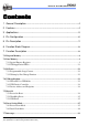
EM78612 Universal Serial Bus Microcontroller 1 General Description·················································································· 4 2 Features··································································································· 4 3 Applications ··············································································································· 5 4 Pin Configuration ··································································································
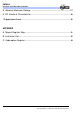
EM78612 Universal Serial Bus Microcontroller 8 Absolute Maximum Ratings···································································· 27 9 DC Electrical Characteristic················································································· 28 10 Application Cricuit···································································································· 30 APPENDIX A.
EM78612 Universal Serial Bus Microcontroller Specification Revision History Doc. Version 1.0 Revision Description Initial Version Product Specification (V1.0) 03.22.
EM78612 Universal Serial Bus Microcontroller 1 General Description The EM78612 is a series of Universal Serial Bus 8-bit RISC microcontrollers. It is specifically designed for USB low speed device application and to support legacy device such as PS/2 mouse. The EM78612 also support one device address and two endpoints.. The EM78612 is implemented on a RISC architecture. It has five-level stack and six interrupt sources. The amount of General Input/Output pins is up to12. Each device has 80 bytes SRAM.
EM78612 Universal Serial Bus Microcontroller • Up to 12 general purposes I/O pins grouped into two ports (Port 6 and 7).
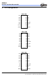
EM78612 Universal Serial Bus Microcontroller 4 Pin Configuration EM78612A P61 1 16 P60 P62 2 15 P64 P63 3 14 P65 P70 4 13 P71 P72 5 12 D+/P50 VSS 6 11 D-/P51 V3.3V 7 10 VDD OSCI 8 9 OSCO EM78612B P60 1 18 P64 P61 2 17 P65 P62 3 16 P66 P63 4 15 P67 P70 5 14 P71 P72 6 13 D+/P50 VSS 7 12 D-/P51 V3.
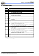
EM78612 Universal Serial Bus Microcontroller 5 Pin Description Symbol I/O Function OSCI I OSCO I/O Return path for 6MHz / 12MHz ceramic resonator. V3.3V O 3.3V DC voltage output from internal regulator. This pin should be tied to a 4.7 F decoupling capacitor to GND. P60 ~ P67 I/O 6MHz / 12MHz ceramic resonator input. Port6 offers up to 8 GIOP pins. P70 ~ P73 I/O The pull high resistors (132K Ohms) and pull low resistors (10K Ohm) are selected through pin programming.
EM78612 Universal Serial Bus Microcontroller 6 Function Block Diagram OSCI Built-in RC OSCO WDT Timer V3.3 D+ 3.
EM78612 Universal Serial Bus Microcontroller After reset Address Program Counter 0x0000 Reset Vector 0x0001 Interrupt Vector 0x000A USB Application Interrupt Vector Page 0 0x03FF 0x0400 Page 1 0x07FF 7.2 Data Memory The Data Memory has 80 bytes SRAM space. It is also equipped with USB Application FIFO space for USB Application. The Figure 7-1 (next page) shows the organization of the Data Memory Space. 7.2.
EM78612 Universal Serial Bus Microcontroller 00 01 02 03 04 R0 R1 R2 R3 R4 (Indirection Addressing Register) (Time Clock / Counter Register) (Program Counter) & Stack (Status Register) (RAM Select Register) 05 06 07 08 09 R5 R6 R7 R8 R9 (Data line I/O Register) (Port 6 I/O Register) (Port 7 I/O Register) (Port6 wakeup pin selection Register) (Port7 wakeup pin selection Register) 0C 0D 0E 0F 10 IOC5 IOC6 IOC7 IOC8 IOCA (Operation mode Control Register) IOCB (Port 6 pull low Control Register) IOCC (P
EM78612 Universal Serial Bus Microcontroller R2 (Program Counter & Stack) Default Value: (0B_0000_0000) The EM78612 Program Counter is an 11-bit long register that allows access to 2K bytes of Program Memory with 5 level stacks. The eight LSB bits, 00~07, are located at R2, while the one MSB bits, 10, is located at R3 [5].The Program Counter is cleared after Power-on reset or WatchDog reset. The first instruction that is executed after a reset is located at Address 00h.
EM78612 Universal Serial Bus Microcontroller R3 [2] Zero flag. It will be set to 1 when the result of an arithmetic or logic operation is zero. R3 [3] Power down flag. It will be set to 1 during Power-on phase or by “WDTC” command and cleared when the MCU enters into Power down mode. It remains in previous state after WatchDog Reset. 1: Power-on. 0: Power down R3 [4] Time-out flag. It will be set to 1 during Power-on phase or by “WDTC” command. It is reset to 0 by WDT time-out.
EM78612 Universal Serial Bus Microcontroller R4 (RAM Select Register) Default Value: (0B_0xxx_xxxx) 7 6 5 4 3 2 1 0 - BK0 Ad5 Ad4 Ad3 Ad2 Ad1 Ad0 R4 (RAM select register) contains the address of the registers. R4 [0~5] are used to select registers in 0x00h~0x3Fh. The address 0x00~0x1F is common space. After 0x1Fh, SRAM is grouped into two banks. R4 [6] are used to select register banks.
EM78612 Universal Serial Bus Microcontroller 0: Enable the wake-up function R9 (Port 7 Wake-up Pin Selection Register) Default Value: (0B_1111_1111) 7 6 5 4 3 2 1 0 - - - - /Wu73 /Wu72 /Wu71 /Wu70 R9 [0 ~ 3] Select which of the Port 7 pins are to be defined to wake-up the MCU from sleep mode. When the state of the selected pins changes during sleep mode, the MCU will wake-up and execute the next instruction automatically.
EM78612 Universal Serial Bus Microcontroller Therefore, before writing data into the FIFO, the firmware will first check this bit to prevent overwriting the existing data. These two bits can only be set by the firmware and cleared by the hardware. RC [7] EP0_W flag. After the UDC completes writing data to the FIFO, this bit will be set automatically. The firmware will clear it as soon as it gets the data from EP0’s FIFO.
EM78612 Universal Serial Bus Microcontroller RF (Interrupt Status Register ) Default Value: (0B_0000_0000) 7 6 - -- RF [0] 5 4 3 2 Port 5 State USB Host USB USB Change_IF Resume_IF Reset_IF Suspend_IF 1 0 EP0_IF TCC_IF TCC Overflow interrupt flag. It will be set while TCC overflows, and is cleared by the firmware. RF [1] EndPoint Zero interrupt flag. It will be set when the EM78612 receives Vender /Customer Command to EndPoint Zero. This bit is cleared by the firmware.
EM78612 Universal Serial Bus Microcontroller CONT (Control Register) 7 6 5 4 3 2 1 0 RW_E /INT TSR2 TSR1 TSR0 PSR2 PSR1 PSR0 NOTE The CONT register can be read by the instruction "CONTR" and written by the instruction “CONTW." CONT [0~2] WatchDog Timer prescaler bits. These three bits are used as the prescaler of WatchDog Timer. CONT [3~5] TCC Timer prescaler bits.
EM78612 Universal Serial Bus Microcontroller IOC5 (Data Line I/O Control Register) Default Value: (0B_0000_0011) 7 6 5 4 3 2 1 0 0 0 0 0 0 0 P51 P50 IOC5 [2~7] Undefined registers. The default value is 0.
EM78612 Universal Serial Bus Microcontroller 1 0 PS/2 Mode 1 1 USB Test Mode IOCA [2~5] Undefined registers. The default value is 0. IOCA [6,7] Select the operation frequency in Dual Clock Mode. Four frequencies are available and can be chosen as Dual Clock mode for running the MCU program. Dual_Frq.1 Dual_Frq.
EM78612 Universal Serial Bus Microcontroller IOCD (Port 7 Pull-High Control Register) Default Value: (0B_0000_0000) 7 6 5 4 3 2 1 0 - - - - PH73 PH72 PH71 PH70 IOCD [0~3] Select whether the 132K Ohm pull-high resistor of Port 7 individual pin is connected or not. 1: Enable the pull-high function. 0: Disable the pull-high function.
EM78612 Universal Serial Bus Microcontroller IOCF (Interrupt Mask Register) Default Value: (0B_0000_0000) 7 6 - - IOCF [0~5] 5 4 Port 5 State USB Host Change_IE Resume_1E 3 USB Reset_IE 2 1 0 USB EP0_IE TCC_IE Suspend_IE TCC / EP0 / USB Suspend / USB Reset / USB Host Resume / Port 5 State Change enable bits.
EM78612 Universal Serial Bus Microcontroller `a\E\ G ? O O b c 7= : ?A@CBED F : ? G BEHJIK@ L LEe T T 798 : 8<;>= : ?A@CBED F : ? G BEHJIK@ T . / 0 1 2 3 4 LEe9L L IM@CL N OMPRQ PCS LEe9L T IM@ T N OMPRQ PCS 5!/ 6 1 2 3 4 .E/ 0 1 2 3 4 5 / 6 1 2 3 4 L L T T U U V V W W 7.
EM78612 Universal Serial Bus Microcontroller Any of the Individual pins of Port 6 and Port 7 can be defined to wakeup the MCU by setting their respective bits, R8 and R9. 7.4 USB Application EM78612 is specially designed for USB device application and has many powerful functions that help the firmware to free itself from complex situation in various aspects of USB application. 7.4.
EM78612 Universal Serial Bus Microcontroller 7.4.2 USB Device Controller The USB Device Controller (UDC) built-in in the EM78612 can interpret the USB Standard Command and response automatically without involving firmware. The embedded Series Interface Engine (SIE) handles the serialization and deserialization of actual USB transmission. Thus, a developer can concentrate his efforts more in perfecting the device actual functions and spend less energy in dealing with USB transaction.
EM78612 Universal Serial Bus Microcontroller C. Special registers and Special Control registers are all set to initial value. The MCU also has a low voltage detector that detects low output power condition. Whenever the output voltage of the 3.3V regulator decreases to below 2.2V, a reset signal is set off. 7.5.2 WatchDog Reset When the WatchDog timer overflows, it causes the WatchDog to reset. After it resets, the program is executed from the beginning and some registers will be reset.
EM78612 Universal Serial Bus Microcontroller : : 7.6.2 Dual Clock Mode The EM78612 has one internal oscillator for power saving application. Clearing the Bit IOCE [7] will enable the low frequency oscillator. At the same time, the external oscillator will be turned off. Then the MCU will run under very low frequency to conserve power. Four types of frequency are available for selection in setting Bits IOCA [6, 7]. The USB Host Resume Interrupt can only be used in this mode.
EM78612 Universal Serial Bus Microcontroller status flags must be cleared by firmware before leaving the interrupt service routine and enabling interrupt. The global interrupt is enabled by the ENI (RETI) instruction and is disabled by the DISI instruction. Interrupt flag. If a bit of RF is asserted, it means the relative interrupt requested. The priority of USB, TCC interrupt is USB > TCC.
EM78612 Universal Serial Bus Microcontroller 9 DC Electrical Characteristic (T = 25 f , VDD = 5V, VSS = 0V) Symble Parameter Condition Min Type Max Unit 3.3V Regulator VRag Output voltage of 3.3v Regulator VDD = 5V 3.0 VResetL Low Power Reset detecting low Voltage - V VResetH Low Power Reset detecting high Voltage - V Ireg 3.3V Regulator driving capacity V3.3 = 3.3V 3.3 - - - - 3.
EM78612 Universal Serial Bus Microcontroller CIN Transceiver Capacitance VRG Output Voltage of Internal Regulator RPH Pull-high resister (D-) - - 20 pF 3.0 - 3.6 V Ki 1.5 Programmable Large Current ISink1 P70, P71 Output Sink Current VOUT = 0.4V, -30% IOC8[0,1] or IOC8[4,5] = 00 3 +30% mA ISink2 P70, P71 Output Sink Current VOUT = 0.4V, -30% IOC8[0,1] or IOC8[4,5] = 01 6 +30% mA ISink3 P70, P71 Output Sink Current VOUT = 0.
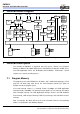
EM78612 Universal Serial Bus Microcontroller 10 Application Cricuit EM78612_CP P60 P64 P61 P65 P62 P66 P63 P67 P70 P71 P72 P73 NA USB Application V3.3 R1 1.5k C3 4.7uF V3.3 VDD OSCI OSCO 1 2 3 4 USB connector Note1. IF IOCA = USB mode, MCU D- pin internal pull-high to V3.3 with 1.5k resistor. P50 D+/CLK D-/DATA J1 P51 P50 Note2. IF IOCA = USB test mode, it is necessary that D- pin external pull-high to V3.3 with 1.5k resistor. V3.3 VSS P51 C1 10uF VDD C2 0.
EM78612 Universal Serial Bus Microcontroller Appendix A.
EM78612 Universal Serial Bus Microcontroller B. Instruction Set Each instruction in the instruction set is a 11-bit word divided into an OP code and one or more operands. All instructions are executed within one single instruction cycle (consisting of 2 oscillator periods), unless the program counter is changed by(a) Executing the instruction "MOV R2,A", "ADD R2,A", "TBL", or any other instructions that write to R2 (e.g. "SUB R2,A", "BS R2,6", "CLR R2", ⋅⋅⋅⋅).
EM78612 Universal Serial Bus Microcontroller INSTRUCTION BINARY HEX MNEMONIC OPERATION STATUS AFFECTED 0 0001 11rr rrrr 01rr DEC R R-1 → R Z 0 0010 00rr rrrr 02rr OR A,R A ∨ VR → A Z 0 0010 01rr rrrr 02rr OR R,A A ∨ VR → R Z 0 0010 10rr rrrr 02rr AND A,R A&R→A Z 0 0010 11rr rrrr 02rr AND R,A A&R→R Z 0 0011 00rr rrrr 03rr XOR A,R A⊕R→A Z 0 0011 01rr rrrr 03rr XOR R,A A⊕R→R Z 0 0011 10rr rrrr 03rr ADD A,R A+R→A Z,C,DC 0 0011 11rr rrrr 03rr ADD R,A A+R→R Z,C,DC
EM78612 Universal Serial Bus Microcontroller INSTRUCTION BINARY HEX MNEMONIC OPERATION STATUS AFFECTED 1 1010 kkkk kkkk 1Akk AND A,k A&k→A Z 1 1011 kkkk kkkk 1Bkk XOR A,k A⊕k→A Z 1 1100 kkkk kkkk 1Ckk RETL k k → A, [Top of Stack] → PC None 1 1101 kkkk kkkk 1Dkk SUB A,k k-A → A Z,C,DC 1 1111 kkkk kkkk 1Fkk ADD A,k k+A → A Z,C,DC Note 1 This instruction is applicable to IOCx only. 2 This instruction is not recommended for RE, RF operation. C.
EM78612 Universal Serial Bus Microcontroller EM78612 has one CODE option registers, which are not part of the normal program memory. The option bits cannot be accessed during normal program execution. 8 7 6 5 R.S. 4 3 Package_ Package_ 1 0 2 OST_1 1 OST_0 0 Frequenc y Bit 0 (Frequency) : Frequency Selection. 0: The MCU run on 12 MHz 1: The MCU run on 6 MHz Bit 2~1 (OST_1 ~ OST_0) : Oscillator Start-up Time. 00: 500us 01: 2ms 10: 8ms 11: 16ms Bit 4~3 (Package_1 ~ Package_0) : Package type selector.