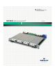
User’s Manual from Emerson Network Power ™ Embedded Computing KAT4000: AMC Carrier for ATCA® April 2007
The information in this manual has been checked and is believed to be accurate and reliable. HOWEVER, NO RESPONSIBILITY IS ASSUMED BY ARTESYN COMMUNICATION PRODUCTS FOR ITS USE OR FOR ANY INACCURACIES. Specifications are subject to change without notice. ARTESYN COMMUNICATION PRODUCTS DOES NOT ASSUME ANY LIABILITY ARISING OUT OF USE OR OTHER APPLICATION OF ANY PRODUCT, CIRCUIT, OR PROGRAM DESCRIBED HEREIN.
Regulatory Agency Warnings & Notices The Emerson KAT4000 meets the requirements set forth by the Federal Communications Commission (FCC) in Title 47 of the Code of Federal Regulations. The following information is provided as required by this agency. This device complies with part 15 of the FCC Rules.
Regulatory Agency Warnings & Notices (continued) EC Declaration of Conformity According to EN 45014:1998 Manufacturer’s Name: Emerson Network Power Embedded Computing Manufacturer’s Address: 8310 Excelsior Drive Madison, Wisconsin 53717 Declares that the following product, in accordance with the requirements of 89/336/EEC, EMC Directive and 99/5/EC, RTTE Directive and their amending directives, Product: ATCA Carrier Model Name/Number: KAT4000/10007505-xx has been designed and manufactured to the
Contents 1 Overview Components and Features . . . . . . . . . . . 1-1 KAT4000 Options. . . . . . . . . . . . . . . . 1-3 Functional Overview . . . . . . . . . . . . . . . . 1-5 Physical Memory Map . . . . . . . . . . . . . . . 1-6 AMC Mapping . . . . . . . . . . . . . . . . . . . . . . 1-9 Additional Information . . . . . . . . . . . . . 1-10 Product Certification . . . . . . . . . . . .1-10 UL Certification . . . . . . . . . . . . . . . . .1-11 RoHS Compliance. . . . . . . . . . . . . . .
Contents (continued) 10 GbE-1 GbE Fat Pipe Switch Module PLD . . . . . . . . . . . . . . . . . . . . . . . . . . . 5-16 Product ID/Version Register. . 5-16 Scratch Register . . . . . . . . . . . .5-17 I2C Register . . . . . . . . . . . . . . . .5-17 Reserved Register 1 . . . . . . . . .5-18 Switch Reset Register . . . . . . . 5-18 Module Status Register . . . . . . 5-19 Switch GPIO Register. . . . . . . . 5-19 GPIN/LED Register . . . . . . . . . .
Contents (continued) Bused Resource Status Command 9-22 Graceful Reset Command. . . . . . . . 9-23 Diagnostic Interrupt Results . . . . .9-24 Get Payload Shutdown Time-Out Command . . . . . . . . . . . . . . . . . . . . . 9-24 Set Payload Shutdown Time-Out Command . . . . . . . . . . . . . . . . . . . . . 9-25 Get Module State Command . . . . . 9-25 Enable AMC Site Command . . . . . . 9-26 Disable AMC Site Command . . . . .9-26 IPMC Watchdog Timer Commands. . . 9-27 Watchdog Timer Actions . . . . . . . .
Contents (continued) Typographic Conventions . . . . . . . 14-9 Boot Commands. . . . . . . . . . . . . . . . . . . 14-9 bootd . . . . . . . . . . . . . . . . . . . . . . . . . 14-9 bootelf . . . . . . . . . . . . . . . . . . . . . . . .14-9 bootm . . . . . . . . . . . . . . . . . . . . . . . .14-9 bootp . . . . . . . . . . . . . . . . . . . . . . . . . 14-9 bootv . . . . . . . . . . . . . . . . . . . . . . . .14-10 bootvx . . . . . . . . . . . . . . . . . . . . . . .14-10 dhcp . . . . . . . . . . . . . .
Contents (continued) Ethernet Switch Configuration . . . . . . . A-2 Default Switch Configuration . . . . . A-2 Serial Command Line Interface (CLI). . . A-3 Log In/Log Out Procedures. . . . . . . . A-3 Help Utility. . . . . . . . . . . . . . . . . . . . . . A-3 Command Hierarchy . . . . . . . . . . . . . A-4 Command Usage Instructions . . . . . A-5 Commands . . . . . . . . . . . . . . . . . . . . . A-5 Command Overview . . . . . . . . . A-6 System Commands . . . . . . . . . . A-8 Console Commands . . . .
(blank page) viii KAT4000 User’s Manual 10007175-02
Figures Figure 1-1: General System Block Diagram. . . . . . . . . . . . . . . . . . . . . . . . . . . . . . . . . . . . . . . . . . . . . . 1-5 Figure 1-2: KAT4000 Memory Map. . . . . . . . . . . . . . . . . . . . . . . . . . . . . . . . . . . . . . . . . . . . . . . . . . . . . 1-6 Figure 1-3: AMC Port Mapping Regions. . . . . . . . . . . . . . . . . . . . . . . . . . . . . . . . . . . . . . . . . . . . . . . . . 1-9 Figure 2-1: Component Map, Top (Rev. 02) . . . . . . . . . . . . . . . . . . . . .
Figures x (continued) KAT4000 User’s Manual Figure 8-2: Diagram of SATA line connections . . . . . . . . . . . . . . . . . . . . . . . . . . . . . . . . . . . . . . . . . . . 8-6 Figure 9-1: IPMC Connections Block Diagram . . . . . . . . . . . . . . . . . . . . . . . . . . . . . . . . . . . . . . . . . . . 9-2 Figure 9-2: Extension Command Request Example. . . . . . . . . . . . . . . . . . . . . . . . . . . . . . . . . . . . . . . 9-7 Figure 9-3: Extension Command Response Example . . . . . . . .
Tables Table 1-1: KAT4000 Address Summary . . . . . . . . . . . . . . . . . . . . . . . . . . . . . . . . . . . . . . . . . . . . . . . . 1-7 Table 1-2: Regulatory Agency Compliance . . . . . . . . . . . . . . . . . . . . . . . . . . . . . . . . . . . . . . . . . . . . 1-10 Table 1-3: Technical References . . . . . . . . . . . . . . . . . . . . . . . . . . . . . . . . . . . . . . . . . . . . . . . . . . . . . 1-12 Table 2-1: Circuit Board Dimensions . . . . . . . . . . . . . . . . . . . . . . . . .
Tables xii (continued) KAT4000 User’s Manual Table 9-10: Get Debug Level Command . . . . . . . . . . . . . . . . . . . . . . . . . . . . . . . . . . . . . . . . . . . . . . . 9-16 Table 9-11: Set Debug Level Command . . . . . . . . . . . . . . . . . . . . . . . . . . . . . . . . . . . . . . . . . . . . . . . . 9-17 Table 9-12: Get Hardware Address Command . . . . . . . . . . . . . . . . . . . . . . . . . . . . . . . . . . . . . . . . . . 9-17 Table 9-13: Set Hardware Address Command . . . . . . .
Tables (continued) Table 11-1: RTC Register Map . . . . . . . . . . . . . . . . . . . . . . . . . . . . . . . . . . . . . . . . . . . . . . . . . . . . . . . . 11-2 Table 12-1: Zone 1 Connector, P10 Pin Assignments . . . . . . . . . . . . . . . . . . . . . . . . . . . . . . . . . . . . 12-1 Table 12-2: Zone 2 Connector, J20 Pin Assignments . . . . . . . . . . . . . . . . . . . . . . . . . . . . . . . . . . . . . 12-3 Table 12-3: Zone 2 Connector, J23 Pin Assignments . . . . . . . . . . . . . . . .
Tables xiv (continued) KAT4000 User’s Manual Table B-23: B3 +12V Current SDR Description . . . . . . . . . . . . . . . . . . . . . . . . . . . . . . . . . . . . . . . . . . B-38 Table B-24: B3 +12V Volt SDR Description . . . . . . . . . . . . . . . . . . . . . . . . . . . . . . . . . . . . . . . . . . . . . B-40 Table B-25: B4 +12V Current SDR Description . . . . . . . . . . . . . . . . . . . . . . . . . . . . . . . . . . . . . . . . . . B-41 Table B-26: B4 +12V Volt SDR Description . . . . . . .
Registers Register 3-1: L2 Control Register (L2CR). . . . . . . . . . . . . . . . . . . . . . . . . . . . . . . . . . . . . . . . . . . . . . . . . . 3-4 Register 3-2: MPC8548 Hardware Implementation Dependent Register 0 (HID0) . . . . . . . . . . . . . 3-6 Register 3-3: MPC8548 Hardware Implementation Dependent Register 1 (HID1) . . . . . . . . . . . . . 3-8 Register 3-4: CPU Machine State Register (MSR) . . . . . . . . . . . . . . . . . . . . . . . . . . . . . . . . . . . . . . . . . .
Registers (continued) Register 7-19: Clock Control Registers 1-14 (CCR1-CCR14) at 0xfc40,0070, 0xfc40,0074, 0xfc40,0078, 0xfc40,007c, 0xfc40,0080, 0xfc40,0084, 0xfc40,0088, 0xfc40,008c, 0xfc40,0090, 0xfc40,0094, 0xfc40,0098, 0xfc40,009c, 0xfc40,00a0, 0xfc40,00a4, respectively . . . . . . . . . . . . . . 7-17 Register 7-20: Clock Synchronizer Interrupt Registers 1-3 (CSI1-CSI3) at 0xfc40,00a8, 0xfc40,00ac, 0xfc40,00b0, respectively . . . . . . . . . . . . . . . . . . . . . . . . . . . . . . . . . . . . . .
Section 1 Overview The KAT4000 is a single-slot Advanced Telecom Computing Architecture (AdvancedTCA®, ATCA™) carrier with up to four Advanced Mezzanine Cards (AMC) expansion modules. This expansion capability enables a wide variety of control and packet processing applications such as WAN access, traffic processing, signaling gateways, media gateways, and many others. ATCA is an open architecture telecom platform as defined by the PICMG® 3.0 Revision 2.0 AdvancedTCA™ Base Specification.
Overview: Components and Features The NOR Flash consists of two 16 megabyte banks. The supported NAND flash is 512 megabytes or 1 gigabyte. Flash is only implemented on the processor KAT4000 board configuration. Chapter 6 provides more information. CPLD: The KAT4000 uses a Complex Programmable Logic Device (CPLD) to control board reset logic, the Board Configuration, Board Revision and User LED registers, and miscellaneous board logic.
Overview: Components and Features with the PICMG® AMC.0 Revision 2.0 Advanced Mezzanine Card Base Specification with the exception of a couple non-conformances. See the KAT4000 Errata for details. Each AMC site is individually configurable. Chapter 8 provides more information.
Overview: Components and Features Fat Pipe Switch Module: A high-speed fat pipe switch is provided as a plug-over module. It supports GbE, Serial Rapid IO (sRIO), PCI Express (PCIe) or 10 Gigabit Ethernet (10 GbE). This switch provides an interconnect between the AMC sites, the ATCA high-speed fabric ports, the processor, the PCIe switch and the Ethernet core switch. See “Fat Pipe Switch Module”, Chapter 5, for information on your module’s configuration.
Overview: Functional Overview FUNCTIONAL OVERVIEW The following block diagram provides a functional overview for the KAT4000: Figure 1-1: General System Block Diagram To Zone 3 (Optional) NAND Flash Main PLD RTC User 1 SEEPROM GbE PHY PCIe (x1 or x4) User 2 SEEPROM GbE To Zone 3 SERDES GbE sRIO (x4) SROM DDR2-667 2GB -48V Cnvrtr Private I2C AMC A-to-D I 2C Clock IPMC I 2C Fat Pipe 3 To Zone 3 RGMII Xfmr Xfmr (2) 2 IPMB Sensors Base 10007175-02 EIA-232 Xcvr Serial Hea
Overview: Physical Memory Map PHYSICAL MEMORY MAP Fig.
Overview: Physical Memory Map Table 1-1 summarizes the physical addresses for the KAT4000 and provides references to more detailed information: Table 1-1: KAT4000 Address Summary Physical Address (hex): Access Mode: Description: FFF0,0000 R/W Boot Area (1 MB) – FF80,0000 – Reserved – See Page: FF70,0000 W – CCSRBAR (MPC8548 Registers, 1 MB) 1 – FC88,0000 Reserved – FC80,0000 R/W Socketed Flash (if installed) (512 KB) 6-1 FC48,0000 – Reserved – FC40,00B0 R/W Clock Synchronizer
Overview: 1-8 Physical Memory Map Physical Address (hex): Access Mode: Description: See Page: (continued) FC40,003C R/W RTM GPIO Control Register (RGCR) 7-7 FC40,0038 R RTM GPIO State Register (RGSR) 7-6 FC40,0034 R/W MISC Control (PCIe, SIO, I2C, Test Clock) Register (MISC) 7-7 FC40,0030 R Boot Device Redirection Register (BDRR) 7-12 FC40,002C R/W Scratch Register 1 (SCR1) 7-8 FC40,0028 W Reset Command Register 2 (RCR2) 7-10 FC40,0024 W Reset Command Register 1 (RCR1) 7-9
Overview: AMC Mapping AMC MAPPING The figure below shows how the KAT4000 maps to the ports defined by the AMC.0 specification: Figure 1-3: AMC Port Mapping Regions Port # Basic Connector Port Mapping ()* ()* " #$ & -()* % & ' +, .
Overview: Additional Information Clocks: This region supports a subset of the clock architecture, as defined in the AMC.0 specification. Common Options: This region supports essential interfaces that are common across multiple Fat Pipe implementations. Fat Pipes: This region supports data path connections including GbE, sRIO, PCIe, and 10 GbE. It can carry large amounts of data without significantly degrading the speed of transmission. Extended Options: This region supports Rear Transition Modules.
Overview: Additional Information Type: Specification: (continued) Environmental NEBS™: Telcordia™ GR-63 (applies to an entire system) – Section 4.3 Equipment Handling Criteria; Section 4.4.1 Earthquake Environment and Criteria (Zone 4); Section 4.4.3 Office Vibration Environment and Criteria; Section 4.4.
Overview: Additional Information (PBDEs) and lead (Pb). Configurations that are RoHS compliant are built with lead-free solder. Configurations that are 5-of-6 are built with tin-lead solder per the lead-in-solder RoHS exemption. To obtain a certificate of conformity (CoC) for the KAT4000 or other modules, send an email to sales@artesyncp.com or call 1-800-356-9602. Have the part number(s) (e.g., C000####-##) for your configuration(s) available when contacting Emerson.
Overview: Additional Information Device / Interface: CPU Document: 3 MPC8548E PowerQUICC III™ Integrated Host Processor Family Preliminary Reference Manual (Freescale® Semiconductor MPC8548ERM Rev. 1: July 2005) http://www.freescale.com EEPROM ATMEL® 2-Wire Serial EEPROM 64K AT24C64B Data Sheet (ATMEL® Corp., Rev. 3350D-SEEPR: May 2005) http://www.atmel.com/literature Ethernet HawX-G26 – 26-Port 10/100/1000 Managed Layer 2 Ethernet Switch, VSC7376 Data Sheet (Vitesse Semiconductor Corp.
Overview: Additional Information Device / Interface: IPMI/IPMB Document: 3 IPMI — Intelligent Platform Management Interface Specification v2.0 (Intel Corp., Hewlett-Packard Co., NEC Corp., Dell Computer Corp., Rev. 1.0; Feb. 12, 2004) IPMB — Intelligent Platform Management Bus Communications Protocol Specification v1.0 (Intel Corp., Hewlett-Packard Co., NEC Corp., Dell Computer Corp., Rev. 1.0; Nov. 15, 1999) IPMI Platform Management FRU Information Storage Definition v1.0 (Intel, Document Revision 1.
Overview: Additional Information 3. Frequently, the most current information regarding addenda/errata for specific documents may be found on the corresponding web site.
(blank page) 1-16 KAT4000 User’s Manual 10007175-02
Section 2 Setup This chapter describes the physical layout of the board and the setup process, including power requirements and environmental considerations. This chapter also includes troubleshooting, service, and warranty information. ELECTROSTATIC DISCHARGE Before you begin the setup process, please remember that electrostatic discharge (ESD) can easily damage the components on the KAT4000 hardware.
Setup: KAT4000 Circuit Board Figure 2-1: Component Map, Top (Rev.
Setup: KAT4000 Circuit Board Figure 2-2: Component Map, Bottom (Rev.
Setup: KAT4000 Circuit Board Front Panel The front panel, shown in Fig. 2-3, consists of four single-width, mid-size Advanced Mezzanine Card (AMC) sites (double-width and compact modules can be accommodated), a hot swap LED, an out of service LED, two user LEDs (see “LEDs” on page 2-10 for more information), and a reset switch. Note: When using a compact AMC module, the module must have a front panel that fully covers the front opening of the KAT4000 to maintain EMC compliance.
Setup: KAT4000 Circuit Board • Zone 3 (ATCA) is for the optional Rear Transition Module (RTM) I/O interconnect—J30 through J33 P10: This connector provides the power and IPMB to the KAT4000. The P10 connector has four levels of sequential mating to provide the proper functionality during live insertion or extraction of the KAT4000. See Table 12-1 for the pin assignments. J20, J23: The 80-pin Zone 2 (ZD) connectors provide three levels of sequential mating.
Setup: KAT4000 Circuit Board Table 2-3: Jumpers–JP2 and JP7 Jumper: JP2 Shunt Description: 1:2 IPMC Mode bit MD2 out-factory use only–used for initial programming of the IPMC controller (default) 3:4 IPMC Mode bit MD1 out-factory use only–used for initial programming of the IPMC controller (default) Register Map: N/A 1:2 Boot from socket in-boot from ROM socket (default) out-boot from soldered flash 3:4 Ignore SROM in-CPU ignores SROM (default) out-CPU loads from SROM JP7 5:6 Boot redirect (see Re
Setup: KAT4000 Circuit Board Figure 2-4: Jumper, Fuse and Switch Locations, Top P1 - CPU JTAG/COP U63 R296 C389 YYYYYY R358 R2088 R356 C2034 C2037 R357 RN60 R1204 RN35 RN62 RN64 RN63 R2120 R335 R331 C467 C454 C450 R2119 R2048 C449 C446 C451 R332 C422 C426 R330 C421 C425 C432 C424 C431 RN34 RN25 L12 R337 L11 C452 R336 L7 C416 RN26 RN30 R302 R313 U70 PHY R301 R312 U65 PHY CR36 U79 CR37 CR38 CR39 1000Base-T SW1 - IPMC Reset C455 R264 SW1 R263 R184 R210
Setup: KAT4000 Circuit Board Figure 2-5: Jumper, Fuse and Switch Locations, Bottom J2000 - Hot Swap Switch Header % )&.
Setup: KAT4000 Circuit Board JTAG Interfaces The KAT4000 provides the capability for JTAG type boundary scan testing. The IPMC controls the two JTAG interfaces (hubs), see Fig. 2-6. One JTAG hub is connected to the fat pipe switch module, two PLDs, and the four AMC sites. The other hub is connected to the Ethernet core switch, the PCI Express switch, the processor, the GbE PHYs, and the synchronization clock circuitry. See Fig. 2-4 and Fig. 2-5 for the location of individual headers.
Setup: KAT4000 Circuit Board JP1: The 10-pin JP1 configuration header is provided for PLD programming. Installing a shunt on JP1, pins 1:2, enables the JP3 PLD programming header. The header pin assignments are defined in Table 7-3. J35: J35 is the 14-pin IPMC JTAG/emulation header. See Table 2-4 for signal descriptions.
>" / ? " ' 1 "6/ @ 1 "6/ @ 1 "6/ @ 1 "6/ @ 1 "6/ @ 1 "6/ < # / ? " ' 1 "6/ : *:+0 : *:+0 : *:+0 : *:+0 : *:+0 : *:+0 : *:+0 : *:+0 : *:+0 : *:+0 : *:+0 : *:+0 PCIe Lane Good & & & ! & & & & & & & & & &! & & & & & & ! & 10007175-02 & & & ; : .* : 2: 0 Status: 10/100 Debug Ethernet ; : .
Setup: KAT4000 Circuit Board Figure 2-8: LEDs, Bottom CR2001 CR2000 CR2002 CR2003 2-12 KAT4000 User’s Manual ; < : 0: %** Hot Swap 0 : %** User 0 : %** User 0 : %**- 0 &: %** B& - , /C Out of Service 10007175-02
Setup: KAT4000 Circuit Board Reset The reset signals are routed to the PLD. See Chapter 7 for the reset registers. The following sources can reset the KAT4000: Front Panel: The front panel reset switch can reset the board. Remote IPMI: The KAT4000 is capable of being reset remotely via the IPMI controller. Software: Software is capable of asserting reset to the individual modules (see “reset” on page 14-25). Processor: The processor is also capable of resetting the board.
Setup: KAT4000 Circuit Board Figure 2-9: KAT4000 Reset Diagram 3_3V 3_3V DEBUG_HRESET* DEBUG_SRESET* DEBUG_TRST* CPU COP/ JTAG % :9& ( 2:* 9& ( 2:& E:* % :(& ( 2:* <:2&(2:* % :2&(2:* <:9& ( 2:* <:(& ( 2:* HRESET_REQ* CPU_TRST* CPU_SRESET* CPU_HRESET* MPC8548 Processor 3_3V (9:&(2:* 1_5V 1_5V 3_3V PWR_OK Voltage Monitor 250mS Delay PWRGD_OR 3_3V 3_3V Front Panel RESET 3_3V POR_RST* Voltage Monitor %( : * OSC_EN Soldered Flash 16/32/64MB Clock Tree 25 MHz 125 MHz 20 MHz 33 MH
Setup: KAT4000 Setup KAT4000 SETUP For step-by-step setup instructions, see the KAT4000 Quick Start Guide, #10008585-xx, or the KAT4000 Quick Start Guide for the No-CPU Carrier Board, #10008506-xx. You need the following items to set up and check the operation of the Emerson KAT4000: ❐ KAT4000 carrier ❐ ATCA chassis and power supply ❐ Compatible AMC modules ❐ Console serial cable(s) ❐ Optional rear transition module and cable ❐ CRT terminal Save the antistatic bag and box for future shipping or storage.
Setup: KAT4000 Setup Power Requirements The KAT4000 draws all payload power from the dual redundant -48 volt inputs on the ATCA connector P10 (Zone 1). Under normal operating conditions, the power requirement is shared between the two -48 volt supplies. Power is limited to 200 watts maximum (including AMC and optional RTM sites), with 80W maximum per site and a combined max of 120W to all four sites and the RTM, if used. Optional RTMs receive their power from the KAT4000.
Setup: Troubleshooting Cooling requirements are a function of operating software, AMC power consumption and AMC airflow resistance. The KAT4000 thermal performance must be verified in the end user’s operating environment. Contact Emerson Technical Support at 1-800-327-1251 for more information.
Setup: Troubleshooting Product Repair If you plan to return the board to Emerson Network Power for service, visit http://www.artesyncp.com/support on the internet or send e-mail to serviceinfo@artesyncp.com to obtain a Return Merchandise Authorization (RMA) number. We will ask you to list which items you are returning and the board serial number, plus your purchase order number and billing information if your KAT4000 hardware is out of warranty.
Section 3 Central Processing Unit This chapter is an overview of the processor logic (optional) on the KAT4000. It includes information on the CPU, exception handling, and the I/O parallel port pin assignments. The KAT4000 uses a Freescale MPC8548 PowerQUICC III™ microprocessor. For more detailed information, refer to the MPC8548E PowerQUICC III™ Integrated Host Processor Family Reference Manual. Refer to Fig. 3-1 for a block diagram of the MPC8548.
Central Processing Unit: Figure 3-1: MPC8548 Block Diagram 0< &2 F%& ' I2C . / "" / ( #6/ > ' I2C . / "" / Serial IRQs DDR2 SDRAM Flash GPIO MII, GMII, TBI, RTBI, RGMII, RMII MII, GMII, TBI, RTBI, RGMII, RMII MII, GMII, TBI, RTBI, RGMII, RMII RTBI, RGMII, RMII . //6 / "" / B . C ; #5 (& ; . /6# #5 5 / #> 6" 00& / "" / / ; 0 #5 / " ;6 # " ;6 / "" / 2( - - +, ( / " & .
Central Processing Unit: MPC8548 Functions MPC8548 FUNCTIONS The MPC8548 provides the following functions on the KAT4000 module.
Central Processing Unit: Microprocessor Core (e500) 4 Poll L2CR[L2I] until it is cleared. 5 Enable the L2 cache for normal operation and then set the L2CR[L2E]. Timer/Counter Each of the four 32-bit wide timer/counters can be selected to operate as a timer or a counter. Each timer/counter increments with every TCLK rising edge. In counter mode, the counter counts down to terminal count, stops, and issues an interrupt.
Central Processing Unit: Microprocessor Core (e500) L2SIZ: L2 SRAM Size—indicates the total available L2 SRAM size (read-only).
Central Processing Unit: Microprocessor Core (e500) L2LFR: L2 cache Lock bits Flash Reset—L2 cache must be enabled for reset to occur (reserved in full memory-mapped SRAM mode). 0 L2 cache lock bits are not cleared or the clear operation completed 1 Reset operation clears each L2 cache line’s lock bits L2LFRID: L2 cache Lock bits Flash Reset select Instruction or Data—indicates whether data, instruction, or both bits are reset.
Central Processing Unit: Microprocessor Core (e500) R: Reserved should be cleared. DOZE: Doze power management mode 0 Doze mode disabled 1 Doze mode enabled NAP: Nap power management mode 0 Nap mode disabled 1 Nap mode enabled SLP: Sleep power management mode enable 0 Sleep mode disabled 1 Sleep mode enabled TBEN: Time Base Enable 0 Time base disabled (no counting) 1 Time base enabled STBCLK: Select Time Base Clock—functions if the time base is enabled.
Central Processing Unit: Interrupts and Exception Processing Register 3-3: MPC8548 Hardware Implementation Dependent Register 1 (HID1) 32 33 34 39 PLL_MODE 48 49 reserved 40 PLL_CFG 50 51 AST ME ABE 45 reserved 46 47 RFXE R 52 63 reserved PLL_MODE: Read-only for integrated devices 01 Fixed value for MPC8548 PLL_CFG: This is reflected directly from configuration input pins (read-only). PLL_CFG[0-4] corresponds to the integer divide ratio and PLL_CFG is the half-mode bit.
Central Processing Unit: Interrupts and Exception Processing Noncritical: The processor is able to change program flow to handle conditions generated by external signals, errors, or unusual conditions. The Save and Restore registers, SRR0/SRR1, save state when they are taken and use the rfi instruction to restore state. The external interrupt enable bit, MSR[EE], can mask these asynchronous interrupts.
Central Processing Unit: Peripheral Interface EE: External interrupt Enable—allows the processor to take external input, fixed-interval timer, system management, performance monitor, or decrementer interrupts.
Central Processing Unit: Priority: Lowest MPC8548 Peripheral Modules Function: Request: (continued) 8 MCC1 receive 9 MCC2 receive 10 MCC1 transmit 11 MCC2 transmit 12 FCC2 receive 13 FCC2 transmit 14 FCC3 receive 15 FCC3 transmit 16 SCC1 receive 17 SCC1 transmit 18 SCC2 receive 19 SCC2 transmit 20 SCC3 receive 21 SCC3 transmit 22 SCC4 receive 23 SCC4 transmit 24 11 IDMA(1-4) Emulation (option 2) 25 SMC1 receive 26 SMC1 transmit 27 SMC2 receive 28 SMC2 transmit
Central Processing Unit: Processor Reset and Clocking Signals Local Bus Controller (LBC) The MPC8548 LBC connects to external memory, DSP and ASIC devices.
Central Processing Unit: MPC8548 Exception Handling SYSCLK: System Clock is the primary clock input to the e500 core and all the devices and interfaces that operate synchronously with the core. RTC: Real-Time Clock is an input to the MPC8548. Optionally, it can be used to clock the e500 core timer facilities and by the MPC8548 PIC global timer facilities. MPC8548 EXCEPTION HANDLING Each type of CPU exception transfers control to a different address in the vector table.
Central Processing Unit: JTAG/COP Interface IVOR: Type: Vector Offset Hex Address: IVOR15 Debug 00F00 Notes: (continued) Caused when a debug exception exists in the DBSR and when DBCR0[IDM]=1 and MSR[DE]=1 JTAG/COP INTERFACE A single JTAG/COP header is provided for debug purposes for the processor. This interface provides for boundary-scan testing of the CPU (see Fig. 3-2) and is compliant with the IEEE 1149.1 standard. The header pin assignments are defined in Table 3-6.
Central Processing Unit: No Processor Configuration Table 3-6: Processor JTAG/COP Pin Assignments (P1) Pin: Signal: Pin: Signal: 1 CPU_TDO 2 Not connected 3 CPU_TDI 4 DEBUG_TRST* 5 Not connected 6 JT_3_ 3V (fused) 7 CPU_TCK 8 Not connected 9 CPU_TMS 10 Not connected 11 DEBUG_SRESET* 12 GND 13 DEBUG_HRESET* 14 Not connected 15 CPU_CKSTP_OUT* 16 GND CPU_CKSTP_OUT*: Checkstop Output—when asserted, this output signal indicates that the CPU has detected a checkstop conditio
(blank page) 3-16 KAT4000 User’s Manual 10007175-02
Section 4 Common Switch Region The KAT4000 supports multiple interfaces. This chapter describes the Ethernet core switch, switch configuration, Ethernet address and PCI Express switch. The board area network (BAN) refers to the routing of the Ethernet ports using the Vitesse VSC7376 Gigabit Ethernet (GbE) core switch or the PCIe ports using the PEX 8524 PCI Express switch.
Common Switch Region: Ethernet Core Switch (optional) ETHERNET CORE SWITCH (OPTIONAL) The optional Vitesse VSC7376 GbE switch is a multilayer switch with 26 tri-speed (10/100/1000 Mbps) SGMII Ethernet ports and integrated 1000Base-BX (SerDes) interfaces. The GbE switch supports the following: • Two SGMII Ethernet ports connected from the switch to the ATCA backplane base fabric via PHYs (PICMG 3.
Common Switch Region: Ethernet Core Switch (optional) Figure 4-2: VSC7376 GbE Switch Block Diagram Frame Bus one for each front port Policer Categorizer Shaper Rewriter Shared RX and TX FIFO Port Block Port Block Shared RX and TX FIFO Policer Categorizer Analyzer/Arbiter Shaper Rewriter 8051 CPU (iCPU) RS232 Interface Serial Interface Parallel Interface MII Management Interface Control/Status Registers RS232 MIIM GPIO 10/100/1000 MAC SGMII/SerDes 10/100/1000 MAC SGMII/SerDes SI PI or
Common Switch Region: Ethernet Core Switch (optional) On-Board Path Device Settings Caution: On-board device values are determined by Emerson. Do not change these values. Altering on-board device values could cause system failure. ! Note: Proprietary information regarding register function or effect is not available in this user’s manual. Please contact the PHY or switch manufacturer directly for details. Table 4-1 lists the KAT4000 PHYs and their respective addresses.
Common Switch Region: Ethernet Address for the KAT4000 Table 4-3 shows the GbE fat pipe’s Ethernet switch default off-board ports. Table 4-3: GbE Fat Pipe Module Ethernet Switch Off-Board Ports Destination: Port: AMC1 22,23,24,25 AMC2 18,19,20,21 AMC3 8,9,10,11 AMC4 14,15,16,17 Fabric Channel 1 4,5,6,7 Fabric Channel 2 0,1,2,3 Ethernet Transceivers The Marvell 88E1111 gigabit Ethernet transceivers are used to interface between the processor MACs and the Ethernet switch ports.
Common Switch Region: Ethernet Address for the GbE Fat Pipe Table 4-4: Ethernet Port Address Numbering Offset: MAC: Byte 5 15:0 Byte 4 Byte 3 Byte 2 23:16 47:24 Description: Ethernet Identifier (Hex): LSB of (serial number -1000) — MSB of (serial number -1000) — Port 4 (eTSEC4) 95 Port 3 (eTSEC3) 94 Port 2 (eTSEC2) 93 Port 1 (eTSEC1) 92 Assigned to Artesyn by IEEE F9 Byte 1 80 Byte 0 00 The last pair of hex numbers correspond to the following formula: n — 1000, where n is the
Common Switch Region: PCI Express Switch (optional) PCI EXPRESS SWITCH (OPTIONAL) The optional PLX Technology, Inc. PEX 8524 PCI Express switch device contains 24 PCI Express lanes and up to six ports. The PCIe switch supports the following: • One port connected from each AMC site to the switch (AMC.0 and AMC.
Common Switch Region: PCI Express Switch (optional) PCI Express Interface Figure 4-3: PEX 8524 Block Diagram Station 0 Lanes Station 1 Ingress Scheduler Egress Scheduler Crossbar Switch Ingress Crossbar Switch Egress Lanes Port 0 PCI Express Upstream Station 0 Non-Blocking Crossbar Switch Fabric PCI Express Downstream Station 1 Crossbar Switch Egress Crossbar Switch Ingress Egress Scheduler Ingress Scheduler The stations implement the PCI Express Base 1.
Common Switch Region: PCI Express Switch (optional) EEPROM Interface The PEX 8524 has an embedded 64-kilobyte SPI EEPROM controller. This direct interface provides the 7.8 MHz serial clock (EE_SK), chip select (EE_CS*), and data output (EE_DO) for the EEPROM; and receives data input (EE_DI) from the EEPROM. Figure 4-4: PEX 8524 SPI EEPROM Interface +3.3 V +3.
(blank page) 4-10 KAT4000 User’s Manual 10007175-02
Section 5 Fat Pipe Switch Module The fat pipe switch module is a plug-over module that provides a high-speed interconnect between the AMC modules, the ATCA high-speed fabric ports, the processor, and the Ethernet core switch or the PCIe switch on the KAT4000. There are four configurations of the fat pipe switch module: GbE, 10 GbE-1 GbE, 10 GbE-10 GbE and sRIO. Note: The 10 GbE-10 GbE and sRIO modules are not yet available for order.
Fat Pipe Switch Module: GbE Fat Pipe Switch Module GBE FAT PIPE SWITCH MODULE Fig. 5-1 shows how the GbE fat pipe switch module maps to ports defined by the AMC.0 specification; see Fig. 1-3 for the full port mapping diagram. Figure 5-1: AMC Port Map Fat Pipes Region–GbE Port Mapping Port # Basic Connector +, +, +, +, & ' 0 1 +, (4 #5 6" . " Fat Pipes: This region supports data path connections such as GbE.
Fat Pipe Switch Module: GbE Fat Pipe Switch Module The following block diagram provides a functional overview for the GbE fat pipe switch module: Figure 5-3: GbE Fat Pipe Switch Module Block Diagram Switch SRAM* Flash* Power Supplies (2) Clock Clock VSC7376 26-port GbE Switch PLD SEEPROM JTAG (8) GbE ports SPI Management Interface 8-bit data bus Address bus GPIO I2C SDA/SCL GPIO (18) GbE ports 120-pin high-speed connector = 25 (4 #5 (& " 5 / "> ? " ," 4 5 5 7 < 2
Fat Pipe Switch Module: GbE Fat Pipe Switch Module GbE Fat Pipe Switch Module Circuit Board The following figures show the component maps for the GbE fat pipe switch module circuit board. C1 C2 Y1 R2 J1 R1 C3 Figure 5-4: GbE Fat Pipe Switch Module Component Map, Top (Rev.
Fat Pipe Switch Module: GbE Fat Pipe Switch Module Components and Features The following is a summary of the GbE fat pipe switch module hardware components and features: VSC7376, HawX-G26 GbE Switch: The Vitesse VSC7376 GbE switch is a multilayer switch with 26 tri-speed (10/100/1000 Mbps) SGMII Ethernet ports and integrated 1000Base-BX (SerDes) interfaces. It is located from FC16,0000-FC17,FFFF. This type of switch is also used on the KAT4000 board.
Fat Pipe Switch Module: GbE Fat Pipe Switch Module J1 is a 120-pin high-speed connector that provides an interface to the four AMC sites, the Ethernet core switch and an 88E1111 Gigabit PHY. J2 is a 180-pin high-speed connector that provides an interface to the RTM channel, clock, PLD, processor, and Zone 2 via fabric channels 1 and 2. Reset: Reset of the GbE fat pipe switch is shown in Fig. 5-7.
Fat Pipe Switch Module: GbE Fat Pipe Switch Module Register 5-1: Product ID/Version Register (PIDV) at 0x00 7 6 5 4 3 2 1 0 PID3 PID2 PID1 PID0 PVER1 PVER0 HVER1 HVER0 PID3–PID0: Product ID 0000 Fat Pipe Module, GbE 0001 Fat Pipe Module, sRIO 0010 Fat Pipe Module, 10 GbE-1 GbE 0011 Fat Pipe Module, 10 GbE-10 GbE (All other values are reserved) PVER1, PVER0: PLD Version 00 Revision 00 HVER1, HVER0: Hardware Version 00 Revision 00 Scratch Register The Scratch register can be used by softwar
Fat Pipe Switch Module: GbE Fat Pipe Switch Module SCL: SCL Control 0 Drives logic “0” on the I2C clock line 1 Tristates I2C clock line (pulled high externally) ADD1, ADD0: I2C Address Values in these bits drive address to I2C ROM Signal Detect Register The Signal Detect register drives the signal detect signals on the VSC7376 Ethernet switch. Default is 0x00.
Fat Pipe Switch Module: GbE Fat Pipe Switch Module Register 5-6: Module Status Register (STAT) at 0x05 7 6 5 reserved 4 3 2 1 0 CPU S2V5 S1V2 INT1 INT0 R: Reserved CPU: Switch Mode 0 Internal 8051 microcontoller disabled, parallel interface used for management access 1 Internal 8051 microcontroller enabled S2V5: 2.5V Power Supply Status 0 Power supply out of spec 1 Power supply within spec S1V2: 1.
Fat Pipe Switch Module: GbE Fat Pipe Switch Module Register 5-8: GPIN/LED Register (GPLED) at 0x07 7 6 5 4 3 2 1 0 GPIO2 GPIO1 GPIO0 RSVD LED3 LED2 LED1 LED0 GPIO2–GPIO0: General Purpose Input from VSC7376 RSVD: Reserved LED3–LED0: LED State 0 Off 1 On 5-10 KAT4000 User’s Manual 10007175-02
Fat Pipe Switch Module: 10 GbE-1 GbE Fat Pipe Switch Module 10 GBE-1 GBE FAT PIPE SWITCH MODULE Fig. 5-8 shows how the 10 GbE-1 GbE fat pipe switch module maps to ports defined by the AMC.0 specification; see Fig. 1-3 for the full port mapping diagram. Figure 5-8: AMC Port Map Fat Pipes Region–10 GbE-1 GbE Port Mapping Port # Basic Connector +, +, +, +, & ' 0 1 +, 7 +, (4 #5 6" .
Fat Pipe Switch Module: 10 GbE-1 GbE Fat Pipe Switch Module The following block diagram provides a functional overview for the 10 GbE-1 GbE fat pipe switch module: Figure 5-10: 10 GbE-1 GbE Fat Pipe Switch Module Block Diagram Clocks (2) I2C SDA/SCL LED Interface 8-bit data bus Address bus GPIO SDA/SCL JTAG PCI Management Interface (3) 10 GbE ports GPIO PLD Clock BCM56580 16-port GbE/ 4-port 10 GbE Switch (17) GbE ports 120-pin high-speed connector Power Supplies (2) Power Supply PEX8111
Fat Pipe Switch Module: 10 GbE-1 GbE Fat Pipe Switch Module 10 GbE-1 GbE Fat Pipe Switch Module Circuit Board The following figures show the component maps for the 10 GbE-1 GbE fat pipe switch module circuit board.
Fat Pipe Switch Module: 10 GbE-1 GbE Fat Pipe Switch Module Components and Features The following is a summary of the 10 GbE-1 GbE fat pipe switch module hardware components and features: BCM56580 10 GbE-1 GbE Switch: The Broadcom BCM56580 is a Layer 2 and 3 network switch with sixteen GbE ports and four 10 GbE ports. The switch uses integrated XAUI SerDes for the 10 GbE ports to the ATCA fabric channels and a single SerDes lane for each 1 GbE port to the AMC modules, complying with the CX-4 and PICMG 3.
Fat Pipe Switch Module: 10 GbE-1 GbE Fat Pipe Switch Module PEX 8111 PCIe to PCI Bridge: The BCM56580 switch is managed by the PCIe connection from the MPC8548 via the PEX8111 bridge chip. The PCIe to PCI bridge supports forward and reverse transparent bridging between the PCIe and PCI buses. The bridge’s PCI Express port has a single x1 link with a maximum throughput of 250 MB/sec per transmit and receive direction. The PEX 8111 is compliant with the PCI Local Bus Specification (rev. 3.
Fat Pipe Switch Module: 10 GbE-1 GbE Fat Pipe Switch Module Figure 5-14: 10 GbE-1 GbE Fat Pipe Switch Reset BCM_PCI_RESET* RESET* PLD BCM56580 10 GbE-1 GbE Switch BCM_TRST* PEX_PCI_RESET*1 PCIE_RST* / 5 2 1asserted with PCIE_RST or for PCI Express Hot Reset or when PCI Express link is down PEX8111 Bridge 10 GbE-1 GbE Fat Pipe Switch Module PLD The PLD is used to interface to the BCM56580 switch. Table 5-3 lists the 8-bit PLD registers followed by the register bit descriptions.
Fat Pipe Switch Module: 10 GbE-1 GbE Fat Pipe Switch Module PID3–PID0: Product ID 0000 Fat Pipe Module, GbE 0001 Fat Pipe Module, sRIO 0010 Fat Pipe Module, 10 GbE-1 GbE 0011 Fat Pipe Module, 10 GbE-10 GbE (All other values are reserved) PVER1, PVER0: PLD Version 00 Revision 00 HVER1, HVER0: Hardware Version 00 Revision 00 Scratch Register The Scratch register can be used by software for reads and writes. Accessing this register does not have any affect on operations. Default is 0x00.
Fat Pipe Switch Module: 10 GbE-1 GbE Fat Pipe Switch Module SCLC: SCL Control 0 Drives logic “0” on the I2C clock line 1 Tristates I2C clock line (pulled high externally) ADD1, ADD0: I2C Address Values in these bits drive address to the Ethernet switch Reserved Register 1 This read-only register is reserved for future use.
Fat Pipe Switch Module: 10 GbE-1 GbE Fat Pipe Switch Module Note: Software must ensure that the switch is held in reset for the minimum amount of time as listed in the Ethernet switch data sheet. Module Status Register The read-only Module Status register contains information relating to the module status, such as power supply state, switch operational mode, and switch interrupt state.
Fat Pipe Switch Module: 10 GbE-1 GbE Fat Pipe Switch Module GPIO3–GPIO0: GPIO State 0 Logic low 1 Logic high GPIN/LED Register The GPIN/LED register controls general purpose inputs to the PLD from the carrier. There are also four LEDs which are under software control.
Fat Pipe Switch Module: 10 GbE-10 GbE Fat Pipe Switch Module 10 GBE-10 GBE FAT PIPE SWITCH MODULE Fig. 5-15 shows how the 10 GbE-10 GbE fat pipe switch module maps to ports defined by the AMC.0 specification; see Fig. 1-3 for the full port mapping diagram. Note: This fat pipe switch module option is currently not available for order.
Fat Pipe Switch Module: sRIO Fat Pipe Switch Module SRIO FAT PIPE SWITCH MODULE Fig. 5-17 shows how the sRIO fat pipe switch module maps to ports defined by the AMC.0 specification; see Fig. 1-3 for the full port mapping diagram. Note: This fat pipe switch module option is currently not available for order. Figure 5-17: AMC Port Map Fat Pipes Region–sRIO Port # Basic Connector Port Mapping &.% &.% & ' 0 1 &.% (4 #5 6" .
Section 6 Memory Configuration The KAT4000 includes the following memory devices: • Two banks of NOR Flash (32 MB total) and one bank of socketed Flash (512 KB) • Up to 1gigabyte of DDR2 Synchronous DRAM (SDRAM) • Up to 1 gigabyte of NAND Flash • Two 8-kilobyte banks of non-volatile serial EEPROM memory BOOT MEMORY CONFIGURATION The KAT4000 boot default is the 8-bit ROM socket which occupies the physical address space beginning at FC80,0000.
Memory Configuration: On-Card SDRAM Caution: When removing socketed PLCC devices, always use an extraction tool designed specifically for that task. Otherwise, you risk damaging the PLCC device. ! The KAT4000 supports a redundant boot bank. This boot bank is automatically used if the primary bank fails to boot properly. The primary and redundant banks are designated from the local processor as well as remotely over IPMI.
Memory Configuration: NVRAM Allocation NVRAM ALLOCATION The KAT4000 uses two eight-kilobyte I2C SROMs for storing non-volatile information such as board, monitor, and operating system configurations, as well as information specific to a user’s application. All Emerson-specific data is stored in the upper two kilobits of each device. The remainder of each device is available for the user’s application. Table 6-2 and Table 6-3 define the organization of data within the SROMs.
(blank page) 6-4 KAT4000 User’s Manual 10007175-02
Section 7 CPLD In addition to reset and interrupt registers, the complex programmable logic device (CPLD) provides the peripheral bus interface for: user LEDs, configuration jumpers, board revision, boot device selection, and the hardware configuration register. The CPLD is in-system programmable (ISP). A single JTAG interface is provided for local programming. Remote programming via the IPMC is also possible. All reset sources and loads are connected to the CPLD.
CPLD: Version and ID Registers Address Offset (hex): Mnemonic: Register Name: Register Map: (continued) 0x60 CSS1 Clock Synchronizer Secondary Source 1 0x64 CSS2 Clock Synchronizer Secondary Source 2 0x68 CSS3 Clock Synchronizer Secondary Source 3 0x6C — Reserved 0x70 CCR1 Clock Control, AMC1 CLK1 0x74 CCR2 Clock Control, AMC1 CLK2 0x78 CCR3 Clock Control, AMC1 CLK3 0x7C CCR4 Clock Control, AMC2 CLK1 0x80 CCR5 Clock Control, AMC2 CLK2 0x84 CCR6 Clock Control, AMC2 CLK3 0x
CPLD: Version and ID Registers PID1, PID0: PID Select 00 KAT4000 01 Reserved 10 Reserved 11 Reserved R: Reserved ECS: Ethernet Core Switch 1 Ethernet Core Switch is installed 0 Ethernet Core Switch is not installed PCIE: PCI Express Switch 1 PCI Express Switch is installed 0 PCI Express Switch is not installed Hardware Version Register (HVR) The read-only Hardware Version register indicates artwork revision and notifies of any other change to the hardware.
CPLD: Configuration Registers CONFIGURATION REGISTERS Hardware Configuration Register 0 (HCR0) The read-only Hardware Configuration 0 register indicates various settings of the particular product configuration. The values of these bits are defined by strapping resistors. Default register values are configuration dependent.
CPLD: Miscellaneous Registers CORE2-0: Core CCB PLL Ratio 000 Reserved 001 Reserved 010 Reserved 011 3:2 100 Reserved 101 5:2 110 3:1 111 Reserved SYS3-0: System CCB PLL Ratio 0000 16:1 1100 12:1 All others are reserved MISCELLANEOUS REGISTERS LED Control Register (LEDR) The KAT4000 has multiple light-emitting diodes (LED) for status and software development (see Section “LEDs” for LED location and description). The LED Control register controls the card’s LEDs. Setting (1) the bit enables the LED.
CPLD: Miscellaneous Registers LDM: LED Debug Mode Setting (0) puts the four debug LEDs into user mode allowing software to turn them off/on individually. By default, they are in hardware debug mode and are connected to specific internal/external signals. 1 Debug mode probes are enabled (default) 0 Debug mode probes are disabled DBG3-0: Debug LEDs 1 On 0 Off Jumper Settings Register (JSR) The read-only Jumper Settings register indicates miscellaneous external settings.
CPLD: Miscellaneous Registers RIO7-0: 1 Logic “1" on the net 0 Logic “0" on the net RTM GPIO Control Register (RGCR) The RTM GPIO Control register controls GPIO between the carrier card and the Rear Transition Module (RTM). The GPIO pin buffers are open collector. Set (1) the bit if the RTM will drive the GPIO line to avoid contention. Default register values are shown in the bottom row of the register table.
CPLD: Boot and Reset Registers FWP1: Flash 1 Write Protect 1 Not write protected 0 Write protected FWP0: Flash 0 Write Protect 1 Not write protected 0 Write protected NFWP: NAND Flash Write Protect 1 Write protected 0 Not write protected SDA: I2C SDA Output Driver State Bit state indicates PLD’s output level on the bus SCL: I2C SCL Output Driver State Bit state indicates PLD’s output level on the bus Scratch Register 1 (SCR1) Scratch register 1 can be used as a reading/writing test register.
CPLD: Boot and Reset Registers Register 7-12: Reset Event Register (RER) at 0xfc40,0020 7 6 5 4 3 2 1 0 R SHR WE COPS COPH PAYR R PBR R: Reserved SHR: Software Issued Hard Reset 1 The last reset was caused by a write to the Reset Command register WE: Watchdog Expiration 1 A reset was caused by the expiration of the watchdog timer COPS: MPC8548 COP Soft Reset 1 A COP header soft reset (SRESET) has occurred COPH: MPC8548 COP Hard Reset 1 A COP header hard reset (HRESET) has occurred PAYR: P
CPLD: Boot and Reset Registers CSR1: Clock Synchronizer 1 Reset 1 Reset 0 No reset (default) CSR2: Clock Synchronizer 2 Reset 1 Reset 0 No reset (default) CSR3: Clock Synchronizer 3 Reset 1 Reset 0 No reset (default) PCIE: PCI Express Reset 1 Reset 0 No reset (default) I2C: I2C Bus Reset 1 Reset 0 No reset (default) FSHR: NOR Flash Reset 1 Resets NOR flash to a known state 0 No reset (default) CER: Core Ethernet Reset 1 Reset 0 No reset (default) Reset Command Register 2 (RCR2) Set only one bit in this r
CPLD: Boot and Reset Registers DER: Debug Ethernet Reset 1 Reset 0 No reset (default) BCR: Base Channel Ethernet Reset 1 Reset 0 No reset (default) NFR: NAND Flash Reset 1 Reset 0 No reset (default) R: Reserved Boot Device Redirection Register (BDRR) The read-only Boot Device Redirection register indicates which of the three devices the CPU is using as the boot device. The BDRR also indicates which device was set as the initial boot device (see Fig. 7-1).
CPLD: Boot and Reset Registers Figure 7-1: Boot Device Redirection H & ! Socketed ROM 1:2 Boot from socketdefault 5:6 Boot device redirection is disabled ; ( #$ H6 / & H & & Flash 1 Socketed ROM ! Flash 0 1:2 Boot from soldered flash 5:6 Boot device redirection is enableddefault Initial Register 7-15: Boot Device Redirection Register (BDRR) at 0xfc40,0030 7 BRB 6 5 reserved 4 3 2 1 0 BSJ R SKT FL1 FL0 BRB: Boot Redirected Bit
CPLD: Clock Synchronizer Registers CLOCK SYNCHRONIZER REGISTERS Clock Synchronizer Control Registers 1-3 (CSC1—CSC3) The Clock Synchronizer Control registers control the functionality of the clock synchronizer devices. Default is 0x40 for register 1 and 0x00 for registers 2 and 3.
CPLD: Clock Synchronizer Registers Clock Synchronizer Primary Source Registers 1-3 (CPS1—CPS3) The Clock Synchronizer Primary Source registers define the input primary source to the three clock synchronizer devices. Default is 0x00 for register 1, 0x02 for register 2 and 0x04 for register 3.
CPLD: Clock Synchronizer Registers Bit: Input Source: 01101 AMC3 CLK2 01110 AMC3 CLK3 01111 AMC4 CLK1 10000 AMC4 CLK2 10001 AMC4 CLK3 10010 reserved ... 11111 reserved Clock Synchronizer Secondary Source Registers 1-3 (CSS1—CSS3) The Clock Synchronizer Secondary Source registers define the input secondary source to the three clock synchronizer devices. Default is 0x01 for register 1, 0x03 for register 2 and 0x05 for register 3.
CPLD: Clock Synchronizer Registers Bit: Input Source: 00011 aTCA CLK2 B 00100 aTCA CLK3 A 00101 aTCA CLK3 B 00110 AMC1 CLK1 00111 AMC1 CLK2 01000 AMC1 CLK3 01001 AMC2 CLK1 01010 AMC2 CLK2 01011 AMC2 CLK3 01100 AMC3 CLK1 01101 AMC3 CLK2 01110 AMC3 CLK3 01111 AMC4 CLK1 10000 AMC4 CLK2 10001 AMC4 CLK3 10010 reserved ...
CPLD: Clock Synchronizer Registers Clock Control Registers (CCR1—CCR14) The Clock Control registers control the source clock to the various clock destinations. Default is 0x0E for all 14 registers. Default register values are shown in the bottom row of the register table.
CPLD: Clock Synchronizer Registers Clock Control Register: Bit: Input Source: 10001 aTCA CLK3 B 14 10010 Sync #1 - 19.44 MHz — 10011 Sync #1 - 2.048 MHz — 10100 Sync #1 - 1.544 MHz — 10101 8 KHz (see note) — 10110 Sync #2 - 19.44 MHz — 10111 Sync #2 - 2.048 MHz — 11000 Sync #2 - 1.544 MHz — 11001 Sync #3 - 19.44 MHz — 11010 Sync #3 - 2.048 MHz — 11011 Sync #3 - 1.544 MHz — 11100 reserved — reserved — ...
CPLD: JTAG Interface HPI, PPI: Holdover and PLL Lock Loss Pending Interrupt (read-only) 1 Interrupt latched 0 No interrupt latched HS, PS: Holdover and PLL Lock Loss Status (read-only) 1 Indicates synchronizer in holdover/PLL lock loss state 0 Indicates synchronizer not in holdover, PLL locked JTAG INTERFACE The KAT4000 provides a single 10-pin JTAG header (JP3) for in-system programming of onboard PLDs, as well as Altera PLDs on AMC site 1 (see Fig. 7-2).
CPLD: JTAG Interface Figure 7-2: PLD JTAG Diagram AMC 1 Port 1 Config. Header JP1 Programming Header JP3 Master Port 2 SCANSCA112 JTAG Multiplexer SCANSTA112 Port 0 Port 3 JTAG Multiplexer KSL PLD IPMC PLD Port 6 Port 4 Port 5 Fat Pipe Switch Module JP1 is the configuration header for PLD programming. Installing a shunt on jumper JP1, pins 1:2, enables the JP3 PLD programming header. The header pin assignments are defined in Table 7-3.
Section 8 AMC Sites The KAT4000 provides four Advanced Mezzanine Card (AMC) sites capable of supporting the following AMC form factors: single- or double-width; mid-size or compact. Total power of the AMC sites, including optional RTMs, shall not exceed 120 watts. B+ style AMC connectors are used. Each site is individually configurable. Note: When using a compact AMC module, the module must have a front panel that fully covers the front opening of the KAT4000 to maintain EMC compliance.
AMC Sites: AMC Connectors AMC CONNECTORS The connectors for modules B1 through B4 have 170 pins (see Fig. 8-1) and support the Ethernet core switch, the PCI Express Switch, the Fat Pipe Switch module, and Zone 3. Refer to the component map in Fig. 2-1 for the location and orientation of the AMC B+ connectors on the KAT4000. Figure 8-1: AMC B+ Connector AMC SIGNALS The following signals are available on all four connectors. All signals are bi-directional unless stated otherwise.
AMC Sites: AMC Signals Bn_TTIPn/RTIPn+/-: Input (receive) and output (transmit) signals to Zone 3. CLK1+/-: CLOCK 1 Connects to the AMC synchronization clock transceivers. CLK2+/-: CLOCK 2 Connects to the AMC synchronization clock transceivers. EXPn_B_RX4/TX4+/-: Optional test loop to B3 port 8 (B1), B4 (B2), B1 (B3) and B2 (B4), respectively. PCI Express interface port output (transmit) or input (receive) signals differential pairs.
AMC Sites: Pin Assignments PIN ASSIGNMENTS Each connector has 170 pins (see Fig. 8-1) and supports PCIe and GbE signals, the Ethernet core switch, the PCI Express switch, the fat pipe switch module, user I/O configuration signals and Zone 3. Table 8-1: B1-B4 AMC Pin Assignments 8-4 KAT4000 User’s Manual Pin: B1-B4 Signal: Pin: B1-B4 Signal: 1 GND 2 12 V 3 Bn_PS1* 4 3.3 V 5 3.
AMC Sites: Pin Assignments Pin: B1-B4 Signal: Pin: B1-B4 Signal: 67 GND 68 AMCn_TXD7+ 69 AMCn_TXD7- 70 GND 71 Bn_SDA 72 12 V 73 GND 74 Bn_CLK1+ 75 Bn_CLK1- 76 GND 77 Bn_CLK2+ 78 Bn_CLK2- 79 GND 80 Bn_CLK3+ 81 Bn_CLK3- 82 GND 83 GND 84 12 V 85 GND 86 GND 87 EXPn_B_TX4- 88 EXPn_B_TX4+ 89 GND 90 EXPn_B_RX4- 91 EXPn_B_RX4+ 92 GND 93 EXPn_B_TX5- 94 EXPn_B_TX5+ 95 GND 96 EXPn_B_RX5- 97 EXPn_B_RX5+ 98 GND 99 EXPn_B_TX6- 100 EXPn_B_TX6+ 101
AMC Sites: SATA Lines Pin: B1-B4 Signal: Pin: B1-B4 Signal: 145 Bn_TTIP5+ 146 GND 147 Bn_RRING6- 148 Bn_RTIP6+ 149 GND 150 Bn_TRING6- 151 Bn_TTIP6+ 152 GND 153 Bn_RRING7- 154 Bn_RTIP7+ 155 GND 156 Bn_TRING7- 157 Bn_TTIP7+ 158 GND 159 Bn_RRING8- 160 Bn_RTIP8+ 161 GND 162 Bn_TRING8- 163 Bn_TTIP8+ 164 GND 165 TCK 166 TMS 167 TRST* 168 TDO 169 TDI 170 GND SATA LINES This section displays the SATA line connections for AMCs in the KAT4000.
Section 9 System Management The KAT4000 provides an intelligent hardware management system, as defined in the AdvancedTCA® Base Specification (PICMG® 3.0; AMC.0). This system implements an Intelligent Platform Management Controller (IPMC) based on the proprietary BMR-H8S-ATCA® reference design from Pigeon Point Systems.
System Management: IPMC Overview The following block diagram shows the IPMC connections for the KAT4000. Figure 9-1: IPMC Connections Block Diagram Payload Power Enables and AMC Sites (B1-B4): Management Payload Processor Interface Boot Device Select Payload Reset Temperature Sensors < %6 " 2 ( / ! ! < . " 2 ( / < &2 CPU Present .
System Management: IPMI Messaging IPMI MESSAGING All IPMI messages contain a Network Function Code field, which defines the category for a particular command. Each category has two codes assigned to it–one for requests and one for responses. The code for a request has the least significant bit of the field set to zero, while the code for a response has the least significant bit of the field set to one. Table 9-1 lists the network function codes (as defined in the IPMI specification) used by the IPMC.
System Management: IPMI Messaging IPMI Completion Codes All IPMI response messages contain a hexadecimal Completion Code field that indicates the status of the operation. Table 9-2 lists the Completion Codes (as defined in the IPMI specification) used by the IPMC.
System Management: Code: IPMB Protocol Description: (continued) Device-Specific (OEM) Codes 01-7E 01-7E Device specific (OEM) completion codes–command-specific codes (also specific for a particular device and version). Interpretation of these codes requires prior knowledge of the device command set.
System Management: SIPL Protocol • The seventh byte and beyond contain parameters for specific commands (if required). • The final byte is the two’s-complement checksum of all of the message data after the first checksum. An IPMI response message (see Table 9-4) is similar to a IPMI request message. The main difference is that the seventh byte contains the Completion Code, and the eighth byte and beyond hold data received from the controller (rather than data to send to the controller).
System Management: Message Bridging The following figures show an example of an extension command request and response, respectively.
System Management: Message Bridging The KAT4000 IPMC also supports message bridging between the Payload Interface and IPMB-O, which allows the payload to send custom messages to and receive them from other shelf entities, such as the shelf manager. Message bridging is implemented using the Send/Get Message commands and also via LUN 10 of the KAT4000 IPMC.
System Management: Standard Commands sufficient for storing at least three IPMB messages, but may be not enough for a larger number of messages. Taking this into account, the payload software must read messages from the queue as fast as possible, caching them on the on-carrier payload side for further handling, if it is necessary.
System Management: 9-10 KAT4000 User’s Manual Standard Commands Command: (continued) netFn: Set Sensor Hysteresis Sensor/Event 04, 05 00 24 Get Sensor Hysteresis Sensor/Event 04, 05 00 25 LUN: Cmd: Set Sensor Thresholds Sensor/Event 04, 05 00 26 Get Sensor Thresholds Sensor/Event 04, 05 00 27 Set Sensor Event Enable Sensor/Event 04, 05 00 28 Get Sensor Event Enable Sensor/Event 04, 05 00 29 Rearm Sensor Events Sensor/Event 04, 05 00 2A Get Sensor Events Sensor/Eve
System Management: Standard Commands Command: (continued) netFn: Get Power Level PICMG 2C, 2D 00 12 Bused Resource Control (Release, Query, Force, Bus Free) PICMG 2C, 2D 00 17 LUN: Cmd: The IPMC implements many standard IPMI commands. For example, software can use the watchdog timer commands to monitor the system’s health. Normally, the software resets the watchdog timer periodically to prevent it from expiring.
System Management: Vendor Commands VENDOR COMMANDS The IPMC supports additional IPMI commands that are specific to Pigeon Point and/or Emerson. This section provides detailed descriptions of those extensions.
System Management: Vendor Commands commands to provide a response (if necessary). The event notification character is sent in a synchronous manner, and does not appear in the contents of SIPL messages sent to the payload.
System Management: Type: Response Data (continued) Vendor Commands Byte: Data Field: (continued) 7 Bits [4:7] Clock Bus 2 Events These bits indicate pending Clock Bus 2 requests arrived from the shelf manager: 0 Clock Bus 2 Query 1 Clock Bus 2 Release 2 Clock Bus 2 Force 3 Clock Bus 2 Free Bits [0:3] Clock Bus 1 Events These bits indicate pending Clock Bus 1 requests arrived from the shelf manager: 0 Clock Bus 1 Query 1 Clock Bus 1 Release 2 Clock Bus 1 Force 3 Clock Bus 1 Free 8 Bits [4:7] Reserve
System Management: Vendor Commands Type: Byte: Data Field: (continued) Response Data 1 Completion Code 2:4 PPS IANA Private Enterprise ID, MS Byte first 0x00400A = 16394 (Pigeon Point Systems) 5 Bit [7] Echo On If this bit is set, the IPMC enables echo for the given serial interface Bits [6:4] Reserved Bits [3:0] Baud Rate ID The baud rate ID defines the interface baud rate as follows: 0 9600 bps 1 19200 bps 2 38400 bps 3 57600 bps (unsupported) 4 115200 bps (unsupported) Set Serial Interface Pr
System Management: Vendor Commands Get Debug Level Command The Get Debug Level command gets the current debug level of the IPMC firmware.
System Management: Vendor Commands Set Debug Level Command The Set Debug Level command sets the current debug level of the IPMC firmware.
System Management: Vendor Commands Set Hardware Address Command The Set Hardware Address command allows overriding of the hardware address read from hardware when the IPMC operates in (Manual) Standalone mode.
System Management: Vendor Commands Set Handle Switch Command The Set Handle Switch command sets the state of the Hot Swap handle switch in (Manual) Standalone mode.
System Management: Vendor Commands Set Payload Communication Time-Out Command The Set Payload Communication Time-Out command sets the payload communication time-out value. Table 9-17: Set Payload Communication Time-Out Command Type: Byte: Data Field: Request Data 1:3 PPS IANA Private Enterprise ID, MS Byte first 0x00400A = 16394 (Pigeon Point Systems) 4 Payload Time-out Payload communication time-out measured in hundreds of milliseconds. Thus, the payload communication time-out may vary from 0.
System Management: Vendor Commands Reset IPMC Command The Reset IPMC command allows the payload to reset the IPMC over the SIPL.
System Management: Vendor Commands Bused Resource Control Command To send a Bused Resource Control command to the shelf manager, the payload uses the Bused Resource Control command of the SIPL.
System Management: Vendor Commands Table 9-22: Bused Resource Status Command Type: Byte: Data Field: Request Data 1:3 PPS IANA Private Enterprise ID, MS Byte first 0x00400A = 16394 (Pigeon Point Systems) 4 Command Types for Shelf Manager to Board 0 Query if board has control of the bus (0=In control, 1= No control) 1 Release request a board to release control of the bus (0=Ack, 1=Refused, 2=No control) 2 Force board to release control of bus immediately (0=Ack, 1=No control) 3 Bus Free informs boa
System Management: Vendor Commands The IPMC does not reset the payload on receiving the Graceful Reset command or timeout. If the IPMC participation is necessary, the payload must request the IPMC to perform a payload reset. The Graceful Reset command is also used to notify the IPMC about the completion of the payload shutdown sequence.
System Management: Vendor Commands To avoid deadlocks that may occur if the payload software does not respond, the IPMC provides a special time-out for the payload shutdown sequence. If the payload does not send the Graceful Reset command within a definite period of time, the IPMC assumes that the payload shutdown sequence is finished, and sends a Module Quiesced Hot Swap event to the KAT4000 controller.
System Management: Vendor Commands Type: Byte: Data Field: (continued) Response Data 1 Completion Code 2:4 PPS IANA Private Enterprise ID, MS Byte first 0x00400A = 16394 (Pigeon Point Systems) 5 AMC Status 0 0 = AMC site is enabled 1 = AMC site is disabled 1 0 = AMC is not present 1 = AMC is present 2 0 = Management power is disabled 1 = Management power is enabled 3 0 = Management power is bad 1 = Management power is good 4 0 = Payload power is disabled 1 = Payload power is enabled 5 0 = Payload
System Management: IPMC Watchdog Timer Commands Type: Byte: Data Field: (continued) Response Data 1 Completion Code 2:4 PPS IANA Private Enterprise ID, MS Byte first 0x00400A = 16394 (Pigeon Point Systems) IPMC WATCHDOG TIMER COMMANDS The IPMC implements a standardized ‘Watchdog Timer’ that can be used for a number of system time-out functions by System Management Software (SMS) or by the monitor. Setting a time-out value of zero allows the selected time-out action to occur immediately.
System Management: IPMC Watchdog Timer Commands The Timer Use fields indicate: Monitor FRB-2 Time-out: A Fault-resilient Booting, level 2 (FRB-2) time-out has occurred. This indicates that the last system reset or power cycle was due to the system time-out during POST, presumed to be caused by a failure or hang related to the bootstrap processor.
System Management: IPMC Watchdog Timer Commands Monitor Support for Watchdog Timer If a system “Warm Reset” occurs, the watchdog timer may still be running while the monitor executes POST. Therefore, the monitor should take steps to stop or restart the watchdog timer early in POST. Otherwise, the timer may expire later during POST or after the OS has booted.
System Management: IPMC Watchdog Timer Commands Table 9-32: Set Watchdog Timer Command 9-30 KAT4000 User’s Manual Type: Byte: Data Field: Request Data 1 Timer Use [7] 1b=don’t log [6] 1b=don’t stop timer on Set Watchdog Timer command (new for IPMI v1.5) new parameters take effect immediately. If timer is already running, countdown value will get set to given value and countdown will continue from that point. If timer is already stopped, it will remain stopped.
System Management: IPMC Watchdog Timer Commands Type: Byte: Data Field: (continued) Request Data (continued) 4 Timer Use Expiration flags clear (0b=leave alone, 1b=clear timer use expiration bit) [7] reserved [6] reserved [5] OEM [4] SMS/OS [3] OS Load [2] Monitor/POST [1] Monitor FRB-2 [0] reserved 5 Initial countdown value, lsbyte (100 ms/count) Response Data 6 Initial countdown value, msbyte 1 Completion Code 1. Potential race conditions exist with implementation of this option.
System Management: 9-32 KAT4000 User’s Manual IPMC Watchdog Timer Commands Type: Byte: Data Field: (continued) Response Data 1 Completion Code 2 Timer Use [7] 1b=don’t log [6] 1b=timer is started (running) 0b=timer is stopped [5:3] reserved [2:0] timer use (logged on expiration if “don’t log” bit = 0) 000b=reserved 001b=Monitor FRB-2 010b=Monitor/POST 011b=OS Load 100b=SMS/OS 101b=OEM 110b, 111b=reserved 3 Timer Actions [7] reserved [6:4] pretime-out interrupt 000b=none 001b=SMI 010b=NMI/Diagno
System Management: FRU LEDs Data Field: (continued) Type: Byte: Response Data 6 Initial countdown value, lsbyte (100 ms/count) (continued) 7 Initial countdown, msbyte 8 Present countdown value, lsbyte. The initial countdown value and present countdown values should match immediately after the countdown is initialized via a Set Watchdog Timer command and after a Reset Watchdog Timer has been executed.
System Management: FRU LEDs Get FRU LED Properties Command This command allows software to determine which LEDs are under IPMC control. Table 9-35: Get FRU LED Properties Command Type: Byte: Data Field: Request Data 1 PICMG Identifier—indicates that this is a PICMG defined group extension command. Use value 00h. 2 FRU Device ID Response Data 1 Completion Code 2 PICMG Identifier—indicates that this is a PICMG defined group extension command. Use value 00h.
System Management: FRU LEDs Type: Byte: Data Field: (continued) Response Data 1 Completion Code CCh If the LED ID contained in the Request data is not present on the FRU 2 PICMG Identifier—indicates that this is a PICMG defined group extension command. Use value 00h. 3 LED Color Capabilities—when a bit is set, the LED supports the color.
System Management: FRU LEDs Set FRU LED State Command The Set FRU LED State command allows the state of the FRU LEDs to be controlled by the management system. Table 9-37: Set FRU LED State Command 9-36 KAT4000 User’s Manual Type: Byte: Data Field: Request Data 1 PICMG Identifier—indicates that this is a PICMG defined group extension command. Use value 00h.
System Management: Type: Response Data FRU LEDs Byte: Data Field: (continued) 4 LED Function 00h LED off override 01h-FAh LED blinking override FBh Lamp Test state Turn on LED specified in byte 3 for the duration specified in byte 5, then return to the highest priority state.
System Management: FRU LEDs Get FRU LED State Command The Get FRU LED State command allows the state of the FRU LEDs to be controlled by the management system. Table 9-38: Get FRU LED State Command Type: Byte: Data Field: Request Data 1 PICMG Identifier—indicates that this is a PICMG defined group extension command. Use value 00h.
System Management: Type: Entities and Entity Associations Byte: Data Field: (continued) 6 Local Control Color Bits [7:4] Reserved, set to 0 Bits [3:0] 0h Reserved 1h Blue 2h Red 3h Green 4h Amber 5h Orange 6h White 7h-Fh Reserved 7 Override State LED Function—is required if either override state or Lamp Test is in effect.
System Management: Sensors and Sensor Data Records Figure 9-4: IPMB Entity Structure FRU 0 r(82, 0, A0, 0) - PICMG Front Board FHot SwapF sensor (Type F0) FIPMB PhysicalF sensor (Type F1) FInflow TempF sensor (Type 01) FOutflow TempF sensor (Type 01) FF/W ProgressF sensor (Type 0F) r(82, 0 , 03, 0) - Processor FBMC WatchdogF sensor (Type 23) FCPU VoltF sensor (Type 02) r(82, 0, 0A, 0) - Power Supply F-48V VoltF sensor (Type 02) F-48V CurrF sensor (Type 03) F-48V Feed A VoltF sensor (Type 02) F-48V Feed B
System Management: Sensors and Sensor Data Records Sensor Name: (continued) Sensor Type: Event/Reading Type: Entity ID: Entity Instance: Event Gen: B2 Hot Swap PICMG FRU Hot Swap=F0 Sensor-specific Discrete=6F PICMG AMC Module=C1 Devicerelative=62 Yes B3 Hot Swap PICMG FRU Hot Swap=F0 Sensor-specific Discrete=6F PICMG AMC Module=C1 Devicerelative=63 Yes B4 Hot Swap PICMG FRU Hot Swap=F0 Sensor-specific Discrete=6F PICMG AMC Module=C1 Devicerelative=64 Yes IPMB Physical PICMG IPMB
System Management: Sensors and Sensor Data Records Sensor Name: (continued) Sensor Type: Event/Reading Type: Entity ID: Entity Instance: Event Gen: CPU Volt Voltage=02 Threshold=01 Processor=03 Devicerelative=60 Yes B1 +12 Volt Voltage=02 Threshold=01 PICMG AMC Module=C1 Devicerelative=61 Yes B1 +12 Curr Current=03 Threshold=01 PICMG AMC Module=C1 Devicerelative=61 Yes B2 +12 Volt Voltage=02 Threshold=01 PICMG AMC Module=C1 Devicerelative=62 Yes B2 +12 Curr Current=03 Thres
System Management: Sensors and Sensor Data Records Note: Each byte has eight bits.
System Management: FRU Inventory FRU INVENTORY The IPMC stores Field Replaceable Unit (FRU) information in its boot memory (SROM). The data structure contains information such as the product name, part number, serial number, manufacturing date, and E-keying information. Please refer to the IPMI specification for complete details on the FRU data structure. Table 9-41 lists the general contents of the KAT4000’s FRU information.
System Management: E-Keying Item: Description: (continued) Maximum Module Current (Per Site) 7.0 Amps Maximum Internal Current (All Sites) 15.0 Amps E-KEYING This section details the interfaces governed by E-keying and the protocols they support. Specifically, this includes the interfaces implemented by the KAT4000 and the E-keying definition that corresponds to each interface. The IPMC supports E-keying for the KAT4000 per the PICMG® 3.0, Revision 2.0; PICMG® 3.1, Revision 1.0; and AMC.
System Management: E-Keying Description: (continued) Field: Value: Link Grouping ID 00h Independent Channel Link Designator 111101000000b Port 3,2,1,0 Enabled; Fabric Interface; Channel 1 Link Type 01h PICMG 3.1 Ethernet Fabric Interface Link Type Extension 0000b Fixed 1000BASE-BX Link Grouping ID 00h Independent Channel Link Designator 001101000000b Port 1,0 Enabled; Fabric Interface; Channel 1 Link Type 01h PICMG 3.
System Management: Firmware Upgrade FIRMWARE UPGRADE The IPMC firmware upgrade is performed using a set of special upgrade request and reply messages that are delivered to and from the IPMC in the same way as standard IPMI commands (for more information, refer to Intelligent Platform Management Bus Communication Protocol specification). These upgrade commands are collectively referred to as the Upgrade protocol in this specification.
System Management: Firmware Upgrade Type: Byte: Data Field: (continued) Response Data 1 Completion Code 2:4 PPS IANA Private Enterprise ID, MS Byte first 0x00400A = 16394 (Pigeon Point Systems) 5 Upgrade Status 0 IPMC is not in the firmware upgrade mode 1 IPMC is in the firmware upgrade mode but upgrade session has not been opened yet 2 IPMC is in the firmware upgrade mode and an upgrade session has already been opened (must send Firmware Upgrade Start to open it) 6 Upgrade Cause, if the Upgrad
System Management: Firmware Upgrade Firmware Upgrade Prepare Command The Firmware Upgrade Prepare command prepares the IPMC for programming of a new firmware image.
System Management: Firmware Upgrade Table 9-47: Firmware Upgrade Write Command Type: Byte: Data Field: Request Data 1 Specifies the target device that is to be programmed with the data provided in the request body. The offset of the location at which the data is to be programmed to the target devices is a 3byte value supplied in little-endian format.
System Management: Firmware Upgrade This command is only supported by the Boot Loader. If the IPMC firmware receives this command, it sends a reply with the 0xC1 (Invalid Command) completion code.
System Management: Firmware Upgrade 2 The upgrade initiator resends the Firmware Upgrade Start command and the Boot Loader returns a success reply indicating that an upgrade session has been opened. 3 The upgrade initiator issues a Firmware Upgrade Prepare (master H8S flash) command to erase the master H8S flash. The Boot Loader erases the master H8S flash and returns a success reply.
Section 10 Synchronization Clocks The KAT4000 implements a flexible clocking circuit based on a clock selection/holdover chip with a PLD wrapper. This PLD wrapper allows local software control of the source clock selection from these input options: backplane CLK1A/B, backplane CLK2A/B, backplane CLK3A/B, AMCn TCLKA, AMCn TCLKB or AMCn FCLKA. Any of these clock sources can be sent to the following output clocks: backplane CLK3A/B, AMCn TCLKA, AMCn TCLKB or AMCn FCLKA.
Synchronization Clocks: MT9045 and MT9046 Clock All clock circuitry and the synchronization clock interface meets all hard requirements as stated in the latest PICMG3.0 and AMC.0 specifications, as well as those in all relevant AMC subspecifications. • Backplane CLK1A/B and CLK2A/B inputs are Stratum Level 4E and Stratum Level 3 or 3E sources, respectively, from the main system clock source.
Section 11 Real-Time Clock The standard Real-Time Clock (RTC) for the KAT4000 is provided by an M41T00 device from STMicroelectronics. This device has power sense circuitry and uses eight bytes of non-volatile RAM for the clock/calendar function. The M41T00 is powered from the +3.3 volt rail during normal operation, and uses a single, super capacitor which provides a minimum two hour backup. BLOCK DIAGRAM Figure 11-1: M41T00 Real-Time Clock Block Diagram OSC1 OSC0 Oscillator 32.
Real-Time Clock: Clock Operation 7 Years register 8 Control register The M41T00 clock continually monitors the supply voltage (Vcc) for an out of tolerance condition. If Vcc falls below switch-over voltage (Vso), the M41T00: • Terminates an access in progress • Resets the device address counter • Does not recognize inputs (prevents erroneous data from being written) At power-up, the M41T00 uses Vcc at Vso and recognizes inputs.
Real-Time Clock: Clock Operation Day: Day of the week Date: Day of the month OUT: Output level 1 Default at initial power-up 0 FT/OUT (pin 7) driven low when FT is also zero FT: Frequency Test bit 1 When oscillator is running at 32,768 Hz, the FT/OUT pin will toggle at 512 Hz 0 The FT/OUT pin is an output driver (default at initial power-up) S: Sign bit 1 Positive calibration 0 Negative calibration Calibration: Calibration bits The calibration circuit adds or subtracts counts from the oscillator divider c
(blank page) 11-4 KAT4000 User’s Manual 10007175-02
Section 12 Connectors There are multiple connectors on the KAT4000. Reference Fig. 2-1 and Fig. 2-2 for their locations. Whether individual backplane connectors are populated on the KAT4000 depends on the specific product configuration. The backplane connectors, Zones 1 through 3, are described in this chapter. ZONE 1 Connector P10 provides the ATCA Zone 1 power (dual redundant -48V DC) and system management connections.
Connectors: Zone 2 Pin: Signal: Insertion Sequence: 13 IPMBA Clock (SCL port A) third 14 IPMBA Data (SDA port A) third 15 IPMBB Clock (SCL port B) third 16 IPMBB Data (SDA port B) third 17 no connect third 18 no connect third 19 no connect third 20 no connect third 21 no connect third 22 no connect third 23 no connect third 24 no connect third 25 Shelf ground first 26 Logic ground first 27 Enable B fourth 28 Voltage Return A (-48RTNA) first 29 Voltage Re
Connectors: Zone 2 • Six signal pairs (12 pins) are available to support the optional Synchronization Clock Interface (J20) for 8 KHz, 19.
Connectors: Zone 3 • m is the logical slot number (1-16) • p is the polarity (+, -) Table 12-3: Zone 2 Connector, J23 Pin Assignments Row: Interface: 1 Fabric Channel 2 2 3 Fabric Channel 1 4 CD Tx2[2]- Rx2[2]+ Tx0[2]+ Tx0[2]- Rx0[2]+ Rx2[2]Rx0[2]- Tx2[1]+ Tx2[1]- Rx2[1]+ Rx2[1]- Tx0[1]+ Tx0[1]- Rx0[1]+ Rx0[1]- XBC1_TR0+ XBC1_TR0- XBC1_TR1+ XBC1_TR1- Base Ethernet 2 XBC2_TR0+ XBC2_TR0- XBC2_TR1+ XBC2_TR1- na no connect Tx3[2]+ Tx3[2]- Rx3[2]+ Tx1[2]+ Tx1[2]- Rx1[2]+
Connectors: Zone 3 Spare AMC site I/O will all be routed to Zone 3 as generic differential pairs, carrying anything from SerDes to TDM signals to single-ended GPIO signals, and is capable of data rates as high as 3.125 Gbps.
Connectors: Zone 3 Row: EF GH 1 no connect no connect RTM_GPIO3 2 B2_RTIP3 B2_RRING3 RTM_GPIO1 RTM_GPIO2 RTM_GPIO0 3 GIG4_TX+ GIG4_TX- B2_RTIP4 B2_RRING4 4 B2_TTIP6 B2_TRING6 B2_RTIP6 B2_RRING6 5 B2_TTIP8 B2_TRING8 B2_RTIP8 B2_RRING8 6 GIG4_RX+ GIG4_RX- no connect no connect 7 RTM_TX0+ RTM_TX0- B3_RTIP2 B3_RRING2 8 RTM_TX1+ RTM_TX1- no connect no connect 9 B3_TTIP3 B3_TRING3 RTM_TX2+ RTM_TX2- 10 B3_TTIP4 B3_TRING4 RTM_TX3+ RTM_TX3- Table 12-6: Zone 3 Con
Connectors: Zone 3 Figure 12-3: Zone 3 Connector, J33 1 6 D C B A Table 12-7: Zone 3 Connector, J33 Pin Assignments A (AMC4): B (AMC3): C (AMC2): D (AMC1): 1 B4_CONSOLE_TX B3_CONSOLE_TX B2_CONSOLE_TX B1_CONSOLE_TX 2 B4_CONSOLE_RX B3_CONSOLE_RX B2_CONSOLE_RX B1_CONSOLE_RX 3 GND GND GND GND 4 B4_LEDCTRL_TX B3_LEDCTRL_TX B2_LEDCTRL_TX B1_LEDCTRL_TX 5 B4_LEDCTRL_RX B3_LEDCTRL_RX B2_LEDCTRL_RX B1_LEDCTRL_RX 6 12V RTM IPMB_RTM_SDA_ BUFF 3.
(blank page) 12-8 KAT4000 User’s Manual 10007175-02
Section 13 Rear Transition Module The KAT-Z3DB is an optional, single-slot ATCA Rear Transition Module (RTM) providing rear shelf I/O access for the KAT4000. This RTM is for development purposes only. It has not been tested for EMI, EMC or ESD. This RTM connects to the KAT4000’s Zone 3 connectors, J30-J32, and ATCA connector, J33. This chapter describes the physical layout of the RTM and the installation process.
Rear Transition Module: Functional Overview FUNCTIONAL OVERVIEW The following block diagram provides a functional overview for the KAT-Z3DB.
Rear Transition Module: Circuit Board CIRCUIT BOARD The KAT-Z3DB circuit board is a rear transition module assembly. It uses a 6-layer printed circuit board with the following dimensions. Table 13-1: RTM Circuit Board Dimensions Width: Depth: 12.687 in. (322.25 mm) 3.481 in. (88.42 mm) The following figure shows the component map for the KAT-Z3DB circuit board.
Rear Transition Module: Circuit Board Figure 13-2: RTM Component Map, Top (Rev.
Rear Transition Module: Face Plate FACE PLATE The rear face plate includes openings for six 9-pin micro-D connectors and one RJ45 connector for serial I/O (see Fig. 13-1). There are also two reset switches: a board reset and an IPMI reset. CONNECTORS There are several connectors on the KAT-Z3DB (see Fig. 13-2). Descriptions and pin assignments are listed below. Console Serial Ports There are multiple asynchronous console serial ports on the face plate.
Rear Transition Module: Setup Figure 13-4: Standard Console Cable Wiring, #10007665-xx DB9 Connector Micro DB9 Connector 24 / Ethernet Port The face plate has one 10/100BASE-T Ethernet port, P3, for debug purposes that routes through P30 to the GbE Core Switch. This port is not functional with the no-CPU KAT4000 configuration. This is a standard RJ45 connector, with the following pin assignments.
Rear Transition Module: Installation ❐ Card cage and power supply ❐ Computer terminal When you unpack the module, save the antistatic bag and box for future shipping or storage. Identification Numbers Before you install the KAT-Z3DB in a system, you should record the following information: • The board serial number: 711G- _____________________________________ . The board serial number appears on a bar code sticker located at the top of the board near A1 (see Fig. 13-2).
Rear Transition Module: Installation KAT4000’s K2 and K1, respectively. Finally mate the RTM’s P33 to the KAT4000 J33 connector and manually push in the module. 4 Lock the Hot Swap ejector handles.
Section 14 Monitor The KAT4000 monitor is based on the Embedded PowerPC Linux Universal Boot (U-Boot) Project program, available under the GNU General Public License (GPL). For instructions on how to obtain the source code for this GPL program, please visit http://www.artesyncp.com, send an e-mail to support@artesyncp.com, or call Emerson at (800) 327-1251. This chapter describes the monitor’s basic features, operation, and configuration sequences.
Monitor: Command-Line Features The monitor command prompt in Fig. 14-1 is the result of a successful hardware boot of the KAT4000 with a GbE fat pipe switch module. Figure 14-1: Example Monitor Start-up Display for KAT4000 with GbE Fat Pipe Switch Module U-Boot 1.1.4 (Jan Hardware initialization Monitor command prompt 14-2 KAT4000 User’s Manual 9 2007 - 11:15:43)1.01d CPU: 8548_E, Version: 2.0, (0x80390020) Core: E500, Version: 2.
Monitor: Command-Line Features The monitor command prompt in Fig. 14-2 is the result of a successful hardware boot of the KAT4000 with a 10 GbE-1 GbE fat pipe switch module. Figure 14-2: Example Monitor Start-up Display for KAT4000 with 10 GbE-1 GbE Fat Pipe Switch Module U-Boot 1.1.4 (Apr 03 2007 - 15:20:30)1.3d Hardware initialization Monitor command prompt CPU: 8548_E, Version: 2.0, (0x80390020) Core: E500, Version: 2.
Monitor: Basic Operation This prompt is also displayed as an indication that the monitor has finished executing a command or function invoked at the command prompt (except when the command loads and jumps to a user application). The hardware product name, KAT4000, and the current software version number are displayed in the prompt. Prior to the console port being available, the monitor will display a four-bit hexadecimal value on LED1 through LED4 to indicate the power-up status (see Table 14-1). See Fig.
Monitor: Basic Operation Figure 14-3: Power-up/Reset Sequence Flowchart RESET Initialize HID0 Initialize MSR Relocate the MPC8548 CCSRBDR base address Map LAWBARs/ TLBs Invalidate the L2 cache LED 0001 Invalidate and enable the L1 data cache Init. serial port per baudrate environment var. LED 0011 Is module a root complex Yes Enumerate PCI per enumerate environment variable No Display version string Display CPU, board, and bus speed LED 0100 Initialize I2C Init. SDRAM.
Monitor: Monitor Recovery and Updates POST Diagnostic Results The KAT4000 Power-On Self-Test (POST) diagnostic results are stored as a 32-bit value in I2C NVRAM at the offset 0x1DD8-0x1DDB. Errors will also be stored in the Vital Products Data section and FRU user space area for access by other devices. Each bit indicates the results of a specific test, therefore this field can store the results of up to 32 diagnostic tests. Table 142 assigns the bits to specific tests.
Monitor: Monitor Recovery and Updates Recovering the Monitor 1 Make sure that a monitor ROM device is installed in the PLCC socket on the KAT4000. 2 Ensure there is a jumper on JP7, across pins 1 and 2. 3 Issue the following command, where serial_number is the board’s serial number, at the monitor prompt: KAT4000 (1.0) => moninit serial_number moninit will also reset environment variables to the default state.
Monitor: Monitor Command Reference Optionally, save your settings: KAT4000 (1.0) => saveenv TFTP the new monitor (binary) image to memory location 0x100000: KAT4000 (1.0) => tftpboot 100000 path_to_file_on_tftp_server Update the monitor: KAT4000 (1.0) => moninit serial_number 100000 If moninit( ) fails, burn the new monitor to a ROM and follow the recovery steps in the “Recovering the Monitor” section.
Monitor: Boot Commands Command Help Access all available monitor commands by pressing the ? key or entering help. Access the monitor online help for individual commands by typing help . The full command name must be entered to access the online help. Typographic Conventions In the following command descriptions, text in Courier shows the command format. Square brackets [ ] enclose optional arguments, and angled brackets < > enclose required arguments.
Monitor: Boot Commands To use network download commands (e.g., bootp, bootvx, rarpboot, tftpboot), the environment variables listed in Table 14-4 must be configured. To set a static IP, these environment variables must be specified through the command line interface. Table 14-4: Static IP Ethernet Configuration Environment Variable: Description: ipaddr Local IP address for the board. serverip TFTP/NFS server address. netmask Net mask. gatewayip Gateway IP address.
Monitor: Boot Commands Definition: dhcp [loadaddress] [bootfilename] To use the dhcp command, your DHCP server must be configured with the variables designated in Table 14-5. Table 14-5: DHCP Ethernet Configuration Environment Variable: Description: Value2: ipaddr Local IP address for the board. Configured by DHCP. e.g., 192.168.1.1 serverip TFTP/NFS server address. This value must be configured after the DHCP IP address is 3 acquired. e.g., 192.168.1.2 netmask Net mask. Obtained by DHCP.
Monitor: File Load Commands Definition: tftpboot [loadaddress] [bootfilename] FILE LOAD COMMANDS The file load commands load files over the serial port. loadb The loadb command loads a binary file over the serial port. The command takes two optional parameters: offset: The address offset parameter allows the file to be stored in a location different than what is indicated within the binary file by adding the value off to the file’s absolute address.
Monitor: Memory Commands cmp The cmp command compares count objects between addr1 and addr2. Any differences are displayed on the console display. Definition: cmp [.b, .w, .l] addr1 addr2 count cp The cp command copies count objects located at the source address to the target address. Note: If the target address is located in the range of the Flash device, it will program the Flash with count objects from the source address. The cp command does not erase the Flash region prior to copying the data.
Monitor: Memory Commands 00080030: ffff ffff ffff ffff ffff ffff ffff ffff ................ mm The mm command modifies memory one object at a time. Once started, the command line prompts for a new value at the starting address. After a new value is entered, pressing ENTER auto-increments the address to the next location. Pressing ENTER without entering a new value leaves the original value for that address unchanged.
Monitor: Flash Commands 00080020: 00080030: 00080040: 00080050: 00080060: 00080070: ffffffff ffffffff ffffffff ffffffff ffffffff ffffffff ffffffff ffffffff ffffffff ffffffff ffffffff ffffffff ffffffff ffffffff ffffffff ffffffff ffffffff ffffffff ffffffff ffffffff ffffffff ffffffff ffffffff ffffffff ................ ................ ................ ................ ................ ................ FLASH COMMANDS The Flash commands affect the StrataFlash device on the KAT4000 circuit board.
Monitor: EEPROM/I2C Commands protect The protect command enables or disables the Flash sector protection for the specified Flash sector. Protection is implemented using software only. The protection mechanism inside the physical Flash part is not being used. Definition: Protect all of the Flash sectors in the address range from start to end. protect on start end Protect all of the sectors SF (first sector) to SL (last sector) in Flash bank # N.
Monitor: EEPROM/I2C Commands icrc32 The icrc32 computes a CRC32 checksum. Definition: icrc32 chip address[.0, .1, .2] count iloop The iloop command reads in an infinite loop on the specified address range. Definition: iloop chip address[.0, .1, .2] [# of objects] imd The imd command displays the primary I2C bus memory. For example: imd 53 1800.2 100 displays 100 bytes from offset 0x1800 of I2C device 0x53 (right-shifted 7-bit address). The .
Monitor: IPMC Commands imw The imw command writes (fills) memory. Definition: imw chip address[.0, .1, .2] value [count] inm The inm command modifies I2C memory, reads it, and keeps the address. Definition: inm chip address[.0, .1, .2] iprobe The iprobe command probes to discover valid primary I2C bus chip addresses. Definition: iprobe iprobe2 The iprobe command probes to discover valid secondary I2C bus chip addresses.
Monitor: IPMC Commands fru set chassis field := [ type | part | serial ] fru set board field := [ date | maker | name | serial | part | file ] fru set product field := [ maker | name | part | version |serial | asset | file ] fru show fru dump fru load Set data in the internal use area. fru set internal The fru create command loads a default fru image to a blank fru device.
Monitor: Environment Parameter Commands Definition: sensor [probe|read|dump] Sensor probe prints out each sensor number and name. sensor probe Sensor read prints out the sensor reading for sensor. sensor read Sensor dump prints out the raw Sensor Data Record (SDR) information for sensor. sensor dump ENVIRONMENT PARAMETER COMMANDS The monitor uses on-board, non-volatile memory for the storage of environment parameters.
Monitor: Test Commands printenv The printenv command displays all of the environment variables and their current values to the display. Definition: Print the values of all environment variables. printenv Print the values of all environment variable (exact match) ‘name’. printenv name … saveenv The saveenv command writes the environment variables to non-volatile memory.
Monitor: Other Commands um The um command is a destructive memory test. Press the ‘q’ key to quit this test; the monitor completes running the most recent iteration, and exits to the default prompt after displaying cumulative results for the completed iterations. Definition: um [.b, .w, .l] base_addr [top_addr] OTHER COMMANDS This section describes all the remaining commands supported by the KAT4000 monitor. autoscr The autoscr command runs a script, starting at address addr, from memory.
Monitor: Other Commands Definition: Set the date and time. date [MMDDhhmm[[CC]YY][.ss]] Display the date and time. date Reset the RTC device. date reset echo The echo command echoes args to console. Definition: echo [args..] enumpci The enumpci command enumerates the PCIe bus (when the hardware is the PCIe Root Complex in the system). Definition: enumpci go The go command runs an application at address addr, passing the optional argument arg to the called application.
Monitor: Other Commands Definition: isdram addr loop The loop command executes an infinite loop on address range. Definition: loop [.b, .w, .l] address number_of_objects memmap The memmap command displays the board’s memory map layout. Definition: memmap moninit The moninit command resets the NVRAM and serial number, and it writes the monitor to Flash. The KAT4000 must be booted from the boot socket for this command to function in the default state.
Monitor: Other Commands Show the header of PCI device bus.device.function. pci header b.d.f Display the PCI configuration space (CFG). pci display[.b, .w, .l] b.d.f [address] [# of objects] Modify, read, and keep the CFG address. pci next[.b, .w, .l] b.d.f address Modify, automatically increment the CFG address. pci modify[.b, .w, .l] b.d.f address Write to the CFG address. pci write[.b, .w, .l] b.d.f address value phy The phy command reads or writes to the contents of the PHY registers.
Monitor: Other Commands run The run command runs the commands in an environment variable var. Definition: run var [ … ] Use $ for variable substitution; the syntax “$(variable_name)” should be used for variable expansion. Example: => setenv cons_opts console=tty0 console=ttyS0,\$(baudrate) => printenv cons_opts cons_opts=console=tty0 console=ttyS0,$(baudrate) Use the \ character to escape execution of the $ as seen in the setenv command above.
Monitor: Other Commands switch_reg The switch_reg command reads or writes to the Ethernet core switch or fat pipe Ethernet switch registers. The values changed via this command are not persistent and clear after a hard or soft reset. Option values are as follows: switch (core or fp), port (0 - 25), block (1-7), and sub-block (0-15). “R” reads the register contents at the address specified. “W” writes the address value to the register address specified.
Monitor: Environment Variables To show VLANs in use on the fat pipe switch: vlan show fp ENVIRONMENT VARIABLES Press the ‘s’ key on the keyboard during reset to force the default monitor environment variables to be loaded during hardware initialization but before diagnostic testing. Table 14-6 lists the monitor’s standard environment variables. Table 14-6: Standard Environment Variables 14-28 KAT4000 User’s Manual Variable: Default Value: baudrate 9600 Console baud rate.
Monitor: Environment Variables Variable: Default Value: ecc_1bit_report off Select the reporting of single bit, correctable ECC errors to the console (errors of 2 or more bits are always reported). Valid options: on, off enumerate on PCI bus enumeration. Valid options: on, off ethaddr 00:80:F9: 92:00:0000:80:F9: 92:FF:FF KAT4000 board Ethernet address for TSEC_1 port. The last digits are the board serial number in hex.
Monitor: Environment Variables Variable: Default Value: pcie_wait 0 Specifies time to wait until PCIe enumeration occurs. When hit ‘q’ during pcie_wait, no PCIe enumeration will occur and a POST fail flag will be set. Valid options: time in seconds physical_slot undefined ATCA chassis physical slot number of KAT4000 location. Valid options: Not defined in default configuration— reported at bootup from the IPMC powerondiags on Turns POST diagnostics on or off after power-on/reset.
Monitor: Troubleshooting Variable6: Description: (continued) app_lock_size Size of user NOR (soldered) flash protection area. bootverifycmd Sets the U-Boot boot command that is used to execute the primary and secondary application images when using the bootv command. If not defined, bootv uses the U-Boot go command as the default. dhcp-client-id Populates the Client Identifier (Option 61) in the DHCP request Packet. See “dhcp” on page -10.
Monitor: Download Formats DOWNLOAD FORMATS The KAT4000 monitor supports binary and Motorola S-Record download formats, as described in the following sections.
Section 15 Acronym List AMC ASCII ATA ATCA BIOS BDRR BMC Cmd CPU CRT CSA CT DDR2 EC ECC EIA EMC ESD ETSI FCC FRU GbE GMII GNU GPIO GPL I2C IANA IEC IO IPMB IPMC IPMI ISP IVOR JTAG LED Advanced Mezzanine Card American Standard Code for Information Interchange Advanced Technology Attachment Advanced Telecom Computing Architecture or AdvancedTCA Basic Input/output System Boot Device Redirection Register Baseboard Management Controller Command code Central Processing Unit Cathode Ray Tube Canadian Standards
Acronym List: (continued) LPC LUN MAC MMC NEBS netFn OEM OS PCI PCIe PHY PLD POST RMA RMII RTC RTM SATA SDR SDRAM SEL SERDES SGMII SMC SO-DIMM SPI sRIO SROM TBD TDM UART UL USB XAUI 15-2 KAT4000 User’s Manual Low Pin Count Logical Unit Number Medium/media Access Control/controller Module Management Controller Network Equipment-Building System Network Function Code Original Equipment Manufacturer Operating System Peripheral Component Interconnect PCI Express Physical Interface Programmable Logic Device
Section A Appendix A NO-CPU KAT4000 The following block diagram provides a functional overview for the no-CPU KAT4000 board configuration. This configuration includes 256 Kb of SRAM memory used by the internal 8051 microcontroller on the VSC7376 Ethernet core switch for run time code storage. This configuration omits SDRAM and NOR and NAND flash. Also, this configuration may not support some IPMC payload features.
Appendix A: Ethernet Switch Configuration ETHERNET SWITCH CONFIGURATION If a processor is not used on the KAT4000, the Ethernet core switch and GbE fat pipe switch module (optional) are managed by an 8051 microcontroller internal to each switch.
Appendix A: Serial Command Line Interface (CLI) • Mirror: Mirroring is disabled. • IP: IP mode is disabled and no IP address/mask/gateway is configured. To enable the web interface, an IP address must be configured. SERIAL COMMAND LINE INTERFACE (CLI) Through the serial-based switch configuration, you have all the configuration options found in the web application and more.
Appendix A: Serial Command Line Interface (CLI) Console Prompt [] -----Up Console> password ? Syntax: Console Password [] Description: Set or display console password. The empty string (“”) disables the password check. []: Password string of up to 16 characters. Console> Command Hierarchy The CLI is hierarchical with two levels, top level and group level.
Appendix A: Serial Command Line Interface (CLI) Also, at group level use the slash (/) key to refer to a context relative to the top level (e.g., from the system group, enter a /console/configuration command or change context into the console group by entering /console). Command Usage Instructions • Commands are not case-sensitive. • Use the horizontal arrow-keys . and . to move the cursor within the command you are entering.
Appendix A: Serial Command Line Interface (CLI) Command Type: Description: (continued) Comma and/or dash separated VLAN ID list. This type can be used for specifying individual VLAN IDs or a range of VLAN IDs. The keyword ‘none’ can be used to specify an empty VLAN ID list. Example: 1,2,4-6 Internal class of service, 1-8 (highest=1). Comma and/or dash separated user group list. This type can be used for specifying individual user groups or a range of user groups.
Appendix A: Serial Command Line Interface (CLI) VLAN Aware [] [enable|disable] VLAN PVID [] [|none] VLAN Frame Type [] [all|tagged] Aggr Configuration Aggr Add Aggr Delete Aggr Lookup Aggr Mode [smac|dmac|xor] User Group Configuration User Group Add [] User Group Delete User Group Lookup QoS Configuration [] QoS Mode [] [tag|port|diffserv] QoS Default [] []
Appendix A: Serial Command Line Interface (CLI) System Commands System Configuration: Syntax: System Configuration [all] Description: Show system name, software version, hardware version and management MAC address. Optionally show the full configuration. [all]: Show the total switch configuration (Default: System configuration only). System Restore Default:Syntax: System Restore Default [keepIP] Description: Restore factory default configuration.
Appendix A: Serial Command Line Interface (CLI) []: Password string of up to 16 characters. Console Timeout: Syntax: Console Timeout [] Description: Set or show the console inactivity timeout in seconds. The value zero disables timeout. []: Timeout value in seconds, 0, 60-10000. Console Prompt: Syntax: Console Prompt [] Description: Set or show the console prompt string. The empty string (“”) clears the prompt string.
Appendix A: Serial Command Line Interface (CLI) [enable|disable]: Enable/disable flow control (Default: Show flow control mode). Port State: Syntax: Port State [] [enable|disable] Description: Set or show the state for the port. : Port list (Default: All ports). [enable|disable]: Enable/disable port state (Default: Show state).
Appendix A: Serial Command Line Interface (CLI) MAC Add |none [] Description: Add a static MAC address table entry and VLAN ID on ports. : MAC address, 12-digit hex string, optionally separated with dashes or colons (e.g., 010203ABCDEF, 01-02-03-AB-CD-EF or 01:02:03:AB:CD:EF). : Port list. Use ”none” to specify no ports. []: VLAN ID, 1-4095 (Default: 1).
Appendix A: Serial Command Line Interface (CLI) MAC Learning [] Description: Enable/disable MAC table auto-learning. [enable|disable]: Enable or disable MAC table learning (default: disable). VLAN Commands VLANs use port IDs versus the port number (i.e., the physical number of the port). Port numbers (“port #”=”port ID”-1) are used when discussing Ethernet switch ports. For example, VLAN port ID 1 is the same as Ethernet switch port 0.
Appendix A: Serial Command Line Interface (CLI) []: Port list (Default: All ports). [enable|disable]: Enable/disable VLAN awareness (Default: Show awareness). VLAN PVID: Syntax: VLAN PVID [] [|none] Description: Set or show the port VLAN ID. Untagged frames received on the port will be classified to this VLAN ID. Frames classified to this VLAN ID will be sent untagged on the port. []: Port list (Default: All ports).
Appendix A: Serial Command Line Interface (CLI) Description: Lookup and display link aggregation group. : Port list. Aggregations including any of the ports will be shown. Aggregation Mode: Syntax: Aggr Mode [smac|dmac|xor] Description: Set or show link aggregation traffic distribution mode. [smac|dmac|xor]: Aggregation mode, SMAC, DMAC or XOR (Default: Show mode). User Group Commands User groups provide a way other than VLANs for making port groupings.
Appendix A: Serial Command Line Interface (CLI) Description: Show the configured QoS mode, default class and DSCP mapping for the port. []: Port list (Default: All ports). QoS Mode: Syntax: QoS Mode [] [tag|port|diffserv] Description: Set or show the QoS mode for the port. []: Port list (Default: All ports). [tag|port|diffserv]: Enable tag, port or IP differentiated services class of service for the port (Default: Show mode).
Appendix A: Serial Command Line Interface (CLI) []: VLAN tag user priority, 0-7 (Default: Show user priority). QoS Shaper: Syntax: QoS Shaper [] [disable|] Description: Set or show the shaper configuration. []: Port list (Default: All ports). [disable|]: Disable or set leaky bucket rate to a % of the port speed [0%-100%] (Default: Show shaper rate).
Appendix A: Serial Command Line Interface (CLI) IP Configuration Description: Show configured IP address, mask, gateway, VLAN ID and mode. IP Setup: Syntax: IP Setup [ipaddress> [ [ipgateway>]]] [] Description: Set or show IP configuration. []: IP address (Default: Show IP configuration). []: IP subnet mask (Default: Subnet mask for address class). []: Default IP gateway (Default: 0.0.0.0). []: VLAN ID, 1-4095 (Default: 1).
Appendix A: Web Interface Debug Write Register Description: Write value to register address. : Block identifier, 0-7 or 0x0-0x7. : Sub block identifier, 0-15 or 0x0-0xf. : Register address within block, 0-255 or 0x00-0xff. : Register value, 0-4294967295 or 0x00000000-0xffffffff. Debug PHY Read: Syntax: Debug PHY Read [] Description: Read PHY register for port. : Port list.
Appendix A: Web Interface • Configure aggregation groups • Configure QoS • Read and clear statistics counters • Restore system defaults Note: The web interface uses port IDs versus the port number (i.e., the physical number of the port). Port numbers (“port #”=”port ID”-1) are used when discussing Ethernet switch ports. For example, VLAN port ID 1 is the same as Ethernet switch port 0. All operations are password protected. The password must be entered at login.
Appendix A: Web Interface Figure A-2: Web Interface for the Ethernet Core Switch A-20 KAT4000 User’s Manual 10007175-02
Section B Appendix B SENSOR DATA RECORDS This appendix details the KAT4000 IPMI Sensor Data Record (SDR) parameter values from “Sensors and Sensor Data Records” on page 9-40. Table B-1 is a summary of all the KAT4000 SDRs with a link to the detailed sensor record. All values are hexadecimal. The no-CPU KAT4000 configuration includes all of the SDRs listed in Table B-1 with the exception of the following: BMC Watchdog, CPU Volt, and F/W (Firmware) Progress.
Appendix B: Sensor Data Records Sensor Name: Record ID (hex): Table Information: (continued) +12V Volt 001e Table B-32 on page B-54 +12V Current 001f Table B-33 on page B-56 F/W (Firmware) Progress 0020 Table B-34 on page B-58 Table B-2: KAT4000 IPMC SDR Description KAT4000: Value: Parameter: Status: Record ID 0000 — — SDR Version 51 — — Record Type 12 Controller — Record Length 12 — — Device Slave Address 00 — — Channel Number 00 — — Power State Notification / Glo
Appendix B: Sensor Data Records Status: (continued) KAT4000 Records: Value: Parameter: Sensor Initialization 67 Init Scanning — Init Sensor Type — Sensor Capabilities 41 Init Events — Sensor Scanning enabled Event Generation enabled Ignore Sensor no Auto Re-Arm enabled Sensor Hysteresis no hysteresis Sensor Threshold Access no threshold Event Message Control global disable only () — — Sensor Type f0 Event/Reading Type Code 6f Sensor Specific Assertion Event Mask 00ff —
Appendix B: Sensor Data Records KAT4000 Records: Value: Parameter: Status: (continued) Lower Critical Threshold 00 — — Lower Non-Critical Threshold 00 — — Positive-Going Threshold Hyst Value 00 — — Negative-Going Threshold Hyst Value 00 — — OEM 00 — — ID String Type / Length Code c8 — — Table B-4: IPMB Physical SDR Description KAT4000 Records: Value: Parameter: Status: Record ID 0002 — — SDR Version 51 — — Record Type 01 Full Sensor Record — Record Length 38
Appendix B: Sensor Data Records KAT4000 Records: Value: Parameter: Status: (continued) Sensor Units 3 - Modifier Unit 00 Unspecified — Linearization 00 — — M 00 — — M, Tolerance 00 — — B 00 — — B, Accuracy 00 — — Accuracy, Accuracy Exp 00 — — R exp, B Exp 00 — — Analog Characteristic Flags 00 — — Nominal Reading 00 — — Normal Maximum 00 — — Normal Minimum 00 — — Sensor Maximum Reading 00 — — Sensor Minimum Reading 00 — — Upper Non-Recoverable Thr
Appendix B: KAT4000 Records: Value: Parameter: Status: (continued) Entity Instance 60 — — Sensor Initialization 67 Init Scanning — Init Sensor Type — Init Events — Sensor Capabilities 41 Sensor Scanning enabled Event Generation enabled Ignore Sensor no Auto Re-Arm enabled Sensor Hysteresis no hysteresis Sensor Threshold Access no threshold Event Message Control global disable only Sensor Type 23 Watchdog2 — Event/Reading Type Code 6f Sensor Specific — Assertion Event
Appendix B: Sensor Data Records KAT4000 Records: Value: Parameter: Status: (continued) Normal Minimum 00 — — Sensor Maximum Reading 00 — — Sensor Minimum Reading 00 — — Upper Non-Recoverable Threshold 00 — — Upper Critical Threshold 00 — — Upper Non-Critical Threshold 00 — — Lower Non-Recoverable Threshold 00 — — Lower Critical Threshold 00 — — Lower Non-Critical Threshold 00 — — Positive-Going Threshold Hyst Value 00 — — Negative-Going Threshold Hyst Value 00
Appendix B: KAT4000 Records: Value: Parameter: Status: (continued) Sensor Capabilities 69 Ignore Sensor no Auto Re-Arm enabled Sensor Hysteresis hysteresis is settable/readable Sensor Threshold Access threshold is settable/readable Event Message Control global disable only Voltage — Sensor Type 02 Event/Reading Type Code 01 Threshold — Assertion Event Mask 4801 Lower Non-Recoverable Threshold comparison returned Upper Non-Recoverable Going High supported Deassertion Event Mask
Appendix B: Sensor Data Records KAT4000 Records: Value: Parameter: Status: (continued) Normal Maximum d6 — — Normal Minimum c2 — — Sensor Maximum Reading ff — — Sensor Minimum Reading 00 — — Upper Non-Recoverable Threshold f5 — — Upper Critical Threshold 00 — — Upper Non-Critical Threshold 00 — — Lower Non-Recoverable Threshold a3 — — Lower Critical Threshold 00 — — Lower Non-Critical Threshold 00 — — Positive-Going Threshold Hyst Value 02 — — Negative-Going
Appendix B: KAT4000 Records: Value: Parameter: Status: (continued) Sensor Capabilities 69 Ignore Sensor no Auto Re-Arm enabled Sensor Hysteresis hysteresis is settable/readable Sensor Threshold Access threshold is settable/readable Event Message Control global disable only Voltage — Sensor Type 02 Event/Reading Type Code 01 Threshold — Assertion Event Mask 4000 Lower Non-Recoverable Threshold comparison returned Deassertion Event Mask 4000 Lower Non-Recoverable Threshold comp
Appendix B: Sensor Data Records KAT4000 Records: Value: Parameter: Status: (continued) Sensor Minimum Reading 00 — — Upper Non-Recoverable Threshold f4 — — Upper Critical Threshold 00 — — Upper Non-Critical Threshold 00 — — Lower Non-Recoverable Threshold a3 — — Lower Critical Threshold 00 — — Lower Non-Critical Threshold 00 — — Positive-Going Threshold Hyst Value 02 — — Negative-Going Threshold Hyst Value 02 — — OEM 00 — — ID String Type / Length Code c5 — —
Appendix B: KAT4000 Records: Value: Parameter: Status: (continued) Event/Reading Type Code 01 Threshold — Assertion Event Mask 4000 Lower Non-Recoverable Threshold comparison returned Deassertion Event Mask 4000 Lower Non-Recoverable Threshold comparison returned Discrete Reading Mask 3f3f Upper Non-Recoverable Threshold settable Upper Critical Threshold settable Sensor Units 1 B-12 Sensor Data Records 00 Upper Non-Critical Threshold settable Lower Non-Recoverable Threshold set
Appendix B: Sensor Data Records KAT4000 Records: Value: Parameter: Status: (continued) Lower Non-Recoverable Threshold 93 — — Lower Critical Threshold 00 — — Lower Non-Critical Threshold 00 — — Positive-Going Threshold Hyst Value 03 — — Negative-Going Threshold Hyst Value 03 — — OEM 00 — — ID String Type / Length Code c5 — — Table B-9: +1.
Appendix B: KAT4000 Records: Value: Parameter: Status: (continued) Discrete Reading Mask 3f3f Upper Non-Recoverable Threshold settable Upper Critical Threshold settable Sensor Units 1 B-14 Sensor Data Records 00 Upper Non-Critical Threshold settable Lower Non-Recoverable Threshold settable Lower Critical Threshold settable Lower Non-Critical Threshold settable Upper Non-Recoverable Threshold readable Upper Critical Threshold readable Upper Non-Critical Threshold readable Lower N
Appendix B: Sensor Data Records KAT4000 Records: Value: Parameter: Status: (continued) Positive-Going Threshold Hyst Value 03 — — Negative-Going Threshold Hyst Value 03 — — OEM 00 — — ID String Type / Length Code c5 — — Table B-10: +1.
Appendix B: KAT4000 Records: Value: Parameter: Status: (continued) Discrete Reading Mask 3f3f Upper Non-Recoverable Threshold settable Upper Critical Threshold settable Sensor Units 1 B-16 Sensor Data Records 00 Upper Non-Critical Threshold settable Lower Non-Recoverable Threshold settable Lower Critical Threshold settable Lower Non-Critical Threshold settable Upper Non-Recoverable Threshold readable Upper Critical Threshold readable Upper Non-Critical Threshold readable Lower N
Appendix B: Sensor Data Records KAT4000 Records: Value: Parameter: Status: (continued) Positive-Going Threshold Hyst Value 03 — — Negative-Going Threshold Hyst Value 03 — — OEM 00 — — ID String Type / Length Code c5 — — Table B-11: CPU Volt SDR Description KAT4000 Records: Value: Parameter: Record ID 0009 — Status: — SDR Version 51 Sensor Model v1.
Appendix B: KAT4000 Records: Value: Parameter: Status: (continued) Discrete Reading Mask 3f3f Upper Non-Recoverable Threshold settable Sensor Units 1 B-18 Sensor Data Records 00 Upper Critical Threshold settable Upper Non-Critical Threshold settable Lower Non-Recoverable Threshold settable Lower Critical Threshold settable Lower Non-Critical Threshold settable Upper Non-Recoverable Threshold readable Upper Critical Threshold readable Upper Non-Critical Threshold readable Lower N
Appendix B: Sensor Data Records KAT4000 Records: Value: Parameter: Status: (continued) Positive-Going Threshold Hyst Value 03 — — Negative-Going Threshold Hyst Value 03 — — OEM 00 — — ID String Type / Length Code c8 — — Table B-12: Inflow Temp SDR Description KAT4000 Records: Value: Parameter: Status: Record ID 000a — — SDR Version 51 — — Record Type 01 Full Sensor Record — Record Length 36 — — Sensor Owner ID 00 — — Sensor Owner LUN 00 — — Sensor Number 0
Appendix B: Status: (continued) KAT4000 Records: Value: Parameter: Assertion Event Mask 7a95 Lower Non-Recoverable Threshold comparison returned Lower Critical Threshold comparison returned Deassertion Event Mask Discrete Reading Mask Sensor Units 1 B-20 Sensor Data Records 7a95 3f3f 80 Lower Non-Critical Threshold comparison returned Upper Non-Recoverable Going High supported Upper Critical Going High supported Upper Non-Critical Going High supported Lower Non-Recoverable Going L
Appendix B: Sensor Data Records KAT4000 Records: Value: Parameter: Status: (continued) B, Accuracy 00 — — Accuracy, Accuracy Exp 00 — — R exp, B Exp e0 — — Analog Characteristic Flags 07 — — Nominal Reading 16 — — Normal Maximum 37 — — Normal Minimum 00 — — Sensor Maximum Reading 7f — — Sensor Minimum Reading 80 — — Upper Non-Recoverable Threshold 4b — — Upper Critical Threshold 41 — — Upper Non-Critical Threshold 37 — — Lower Non-Recoverable Threshold
Appendix B: Status: (continued) KAT4000 Records: Value: Parameter: Sensor Initialization 7f Init Scanning — Init Sensor Type — Sensor Capabilities 69 Init Hysteresis — Init Thresholds — Init Events — Sensor Scanning enabled Event Generation enabled Ignore Sensor no Auto Re-Arm enabled Sensor Hysteresis hysteresis is settable/readable Sensor Threshold Access threshold is settable/readable Event Message Control global disable only Sensor Type 01 Temperature — Event/Reading
Appendix B: Sensor Data Records KAT4000 Records: Value: Parameter: Status: (continued) Discrete Reading Mask 3f3f Upper Non-Recoverable Threshold settable Upper Critical Threshold settable Sensor Units 1 80 Upper Non-Critical Threshold settable Lower Non-Recoverable Threshold settable Lower Critical Threshold settable Lower Non-Critical Threshold settable Upper Non-Recoverable Threshold readable Upper Critical Threshold readable Upper Non-Critical Threshold readable Lower Non-Rec
Appendix B: Sensor Data Records KAT4000 Records: Value: Parameter: Status: (continued) Positive-Going Threshold Hyst Value 02 — — Negative-Going Threshold Hyst Value 02 — — OEM 00 — — ID String Type / Length Code cc — — Table B-14: Version Change SDR Description KAT4000 Records: Value: Parameter: Status: Record ID 000c — — SDR Version 51 — — Record Type 01 Full Sensor Record — Record Length 39 — — Sensor Owner ID 00 — — Sensor Owner LUN 00 — — Sensor Number
Appendix B: Sensor Data Records KAT4000 Records: Value: Parameter: Status: (continued) M 00 — — M, Tolerance 00 — — B 00 — — B, Accuracy 00 — — Accuracy, Accuracy Exp 00 — — R exp, B Exp 00 — — Analog Characteristic Flags 00 — — Nominal Reading 00 — — Normal Maximum 00 — — Normal Minimum 00 — — Sensor Maximum Reading 00 — — Sensor Minimum Reading 00 — — Upper Non-Recoverable Threshold 00 — — Upper Critical Threshold 00 — — Upper Non-Critical Thre
Appendix B: Status: (continued) KAT4000 Records: Value: Parameter: Sensor Initialization 67 Init Scanning — Init Sensor Type — Sensor Capabilities B-26 Sensor Data Records 41 Init Events — Sensor Scanning enabled Event Generation enabled Ignore Sensor no Auto Re-Arm enabled Sensor Hysteresis no hysteresis Sensor Threshold Access no threshold Event Message Control global disable only — — — Sensor Type f0 Event/Reading Type Code 6f Sensor Specific Assertion Event Mask 00
Appendix B: Sensor Data Records KAT4000 Records: Value: Parameter: Status: (continued) Lower Critical Threshold 00 — — Lower Non-Critical Threshold 00 — — Positive-Going Threshold Hyst Value 00 — — Negative-Going Threshold Hyst Value 00 — — OEM 00 — — ID String Type / Length Code cb — — Table B-16: B2 Hot Swap SDR Description KAT4000 Records: Value: Parameter: Status: Record ID 000e — — SDR Version 51 — — Record Type 01 Full Sensor Record — Record Length 36 —
Appendix B: Sensor Data Records KAT4000 Records: Value: Parameter: Status: (continued) Sensor Units 3 - Modifier Unit 00 Unspecified — Linearization 00 — — M 00 — — M, Tolerance 00 — — B 00 — — B, Accuracy 00 — — Accuracy, Accuracy Exp 00 — — R exp, B Exp 00 — — Analog Characteristic Flags 00 — — Nominal Reading 00 — — Normal Maximum 00 — — Normal Minimum 00 — — Sensor Maximum Reading 00 — — Sensor Minimum Reading 00 — — Upper Non-Recoverable Thr
Appendix B: Sensor Data Records Status: (continued) KAT4000 Records: Value: Parameter: Sensor Initialization 67 Init Scanning — Init Sensor Type — Sensor Capabilities 41 Init Events — Sensor Scanning enabled Event Generation enabled Ignore Sensor no Auto Re-Arm enabled Sensor Hysteresis no hysteresis Sensor Threshold Access no threshold Event Message Control global disable only — — — Sensor Type f0 Event/Reading Type Code 6f Sensor Specific Assertion Event Mask 00ff —
Appendix B: Sensor Data Records KAT4000 Records: Value: Parameter: Status: (continued) Lower Critical Threshold 00 — — Lower Non-Critical Threshold 00 — — Positive-Going Threshold Hyst Value 00 — — Negative-Going Threshold Hyst Value 00 — — OEM 00 — — ID String Type / Length Code cb — — Table B-18: B4 Hot Swap SDR Description KAT4000 Records: Value: Parameter: Status: Record ID 0010 — — SDR Version 51 — — Record Type 01 Full Sensor Record — Record Length 36 —
Appendix B: Sensor Data Records KAT4000 Records: Value: Parameter: Status: (continued) Sensor Units 3 - Modifier Unit 00 Unspecified — Linearization 00 — — M 00 — — M, Tolerance 00 — — B 00 — — B, Accuracy 00 — — Accuracy, Accuracy Exp 00 — — R exp, B Exp 00 — — Analog Characteristic Flags 00 — — Nominal Reading 00 — — Normal Maximum 00 — — Normal Minimum 00 — — Sensor Maximum Reading 00 — — Sensor Minimum Reading 00 — — Upper Non-Recoverable Thr
Appendix B: Status: (continued) KAT4000 Records: Value: Parameter: Sensor Initialization 5d Init Scanning — Init Sensor Type — Sensor Capabilities 69 Init Hysteresis — Init Thresholds — Sensor Scanning enabled Ignore Sensor no Auto Re-Arm enabled Sensor Hysteresis hysteresis is settable/readable Sensor Threshold Access threshold is settable/readable Event Message Control global disable only Current — Sensor Type 03 Event/Reading Type Code 01 Threshold — Assertion Event M
Appendix B: Sensor Data Records KAT4000 Records: Value: Parameter: Status: (continued) Sensor Minimum Reading 00 — — Upper Non-Recoverable Threshold ff — — Upper Critical Threshold 00 — — Upper Non-Critical Threshold 00 — — Lower Non-Recoverable Threshold 00 — — Lower Critical Threshold 00 — — Lower Non-Critical Threshold 00 — — Positive-Going Threshold Hyst Value 03 — — Negative-Going Threshold Hyst Value 00 — — OEM 00 — — ID String Type / Length Code cc — —
Appendix B: Sensor Data Records KAT4000 Records: Value: Parameter: Status: (continued) Deassertion Event Mask 4800 Lower Non-Recoverable Threshold comparison returned Upper Non-Recoverable Going High supported Discrete Reading Mask 3838 Upper Non-Recoverable Threshold settable Upper Critical Threshold settable Sensor Units 1 B-34 00 Upper Non-Critical Threshold settable Upper Non-Recoverable Threshold readable Upper Critical Threshold readable Upper Non-Critical Threshold readabl
Appendix B: Sensor Data Records KAT4000 Records: Value: Parameter: Status: (continued) ID String Type / Length Code cc — — Table B-21: B2 +12V Current SDR Description KAT4000 Records: Value: Parameter: Status: Record ID 0013 — — SDR Version 51 — — Record Type 01 Full Sensor Record — Record Length 37 — — Sensor Owner ID 00 — — Sensor Owner LUN 00 — — Sensor Number 00 — — Entity ID c1 AMC Module — Entity Instance 66 — — Sensor Initialization 5d Init Scannin
Appendix B: Sensor Data Records KAT4000 Records: Value: Parameter: Status: (continued) Sensor Units 3 - Modifier Unit 00 Unspecified — Linearization 00 — — M 8a — — M, Tolerance 40 — — B 00 — — B, Accuracy 00 — — Accuracy, Accuracy Exp 00 — — R exp, B Exp c0 — — Analog Characteristic Flags 07 — — Nominal Reading 66 — — Normal Maximum bf — — Normal Minimum 00 — — Sensor Maximum Reading ff — — Sensor Minimum Reading 00 — — Upper Non-Recoverable Thr
Appendix B: Sensor Data Records Status: (continued) KAT4000 Records: Value: Parameter: Sensor Initialization 5d Init Scanning — Init Sensor Type — Sensor Capabilities 69 Init Hysteresis — Init Thresholds — Sensor Scanning enabled Ignore Sensor no Auto Re-Arm enabled Sensor Hysteresis hysteresis is settable/readable Sensor Threshold Access threshold is settable/readable Event Message Control global disable only Voltage — Sensor Type 02 Event/Reading Type Code 01 Threshold
Appendix B: Sensor Data Records KAT4000 Records: Value: Parameter: Status: (continued) Sensor Minimum Reading 00 — — Upper Non-Recoverable Threshold f0 — — Upper Critical Threshold 00 — — Upper Non-Critical Threshold 00 — — Lower Non-Recoverable Threshold 00 — — Lower Critical Threshold 00 — — Lower Non-Critical Threshold 00 — — Positive-Going Threshold Hyst Value 02 — — Negative-Going Threshold Hyst Value 00 — — OEM 00 — — ID String Type / Length Code cc — —
Appendix B: Sensor Data Records KAT4000 Records: Value: Parameter: Status: (continued) Deassertion Event Mask 4800 Lower Non-Recoverable Threshold comparison returned Upper Non-Recoverable Going High supported Discrete Reading Mask 3838 Upper Non-Recoverable Threshold settable Upper Critical Threshold settable Sensor Units 1 00 Upper Non-Critical Threshold settable Upper Non-Recoverable Threshold readable Upper Critical Threshold readable Upper Non-Critical Threshold readable Ana
Appendix B: Sensor Data Records KAT4000 Records: Value: Parameter: Status: (continued) ID String Type / Length Code cc — — Table B-24: B3 +12V Volt SDR Description KAT4000 Records: Value: Parameter: Status: Record ID 0016 — — SDR Version 51 — — Record Type 01 Full Sensor Record — Record Length 37 — — Sensor Owner ID 00 — — Sensor Owner LUN 00 — — Sensor Number 00 — — Entity ID c1 AMC Module — Entity Instance 67 — — Sensor Initialization 5d Init Scanning
Appendix B: Sensor Data Records KAT4000 Records: Value: Parameter: Status: (continued) Sensor Units 3 - Modifier Unit 00 Unspecified — Linearization 00 — — M 06 — — M, Tolerance 00 — — B 00 — — B, Accuracy 00 — — Accuracy, Accuracy Exp 00 — — R exp, B Exp e0 — — Analog Characteristic Flags 07 — — Nominal Reading c8 — — Normal Maximum d6 — — Normal Minimum 00 — — Sensor Maximum Reading fe — — Sensor Minimum Reading 00 — — Upper Non-Recoverable Thr
Appendix B: KAT4000 Records: Value: Parameter: Status: (continued) Entity Instance 68 — — Sensor Initialization 5d Init Scanning — Init Sensor Type — Sensor Capabilities 69 Init Hysteresis — Init Thresholds — Sensor Scanning enabled Ignore Sensor no Auto Re-Arm enabled Sensor Hysteresis hysteresis is settable/readable Sensor Threshold Access threshold is settable/readable Event Message Control global disable only Current — Sensor Type 03 Event/Reading Type Code 01 Thre
Appendix B: Sensor Data Records KAT4000 Records: Value: Parameter: Status: (continued) Sensor Minimum Reading 00 — — Upper Non-Recoverable Threshold ff — — Upper Critical Threshold 00 — — Upper Non-Critical Threshold 00 — — Lower Non-Recoverable Threshold 00 — — Lower Critical Threshold 00 — — Lower Non-Critical Threshold 00 — — Positive-Going Threshold Hyst Value 03 — — Negative-Going Threshold Hyst Value 00 — — OEM 00 — — ID String Type / Length Code cc — —
Appendix B: Sensor Data Records KAT4000 Records: Value: Parameter: Status: (continued) Deassertion Event Mask 4800 Lower Non-Recoverable Threshold comparison returned Upper Non-Recoverable Going High supported Discrete Reading Mask 3838 Upper Non-Recoverable Threshold settable Upper Critical Threshold settable Sensor Units 1 B-44 00 Upper Non-Critical Threshold settable Upper Non-Recoverable Threshold readable Upper Critical Threshold readable Upper Non-Critical Threshold readabl
Appendix B: Sensor Data Records KAT4000 Records: Value: Parameter: Status: (continued) OEM 00 — — ID String Type / Length Code cc — — Table B-27: -48V Volt SDR Description KAT4000 Records: Value: Parameter: Status: Record ID 0019 — — SDR Version 51 — — Record Type 01 Full Sensor Record — Record Length 34 — — Sensor Owner ID 00 — — Sensor Owner LUN 00 — — Sensor Number 00 — — Entity ID 0a — — Entity Instance 60 — — Sensor Initialization 7f Init Scannin
Appendix B: KAT4000 Records: Value: Parameter: Status: (continued) Discrete Reading Mask 3f3f Upper Non-Recoverable Threshold settable Upper Critical Threshold settable Upper Non-Critical Threshold settable Sensor Units 1 B-46 Sensor Data Records 00 Lower Non-Recoverable Threshold settable Lower Critical Threshold settable Lower Non-Critical Threshold settable Upper Non-Recoverable Threshold readable Upper Critical Threshold readable Upper Non-Critical Threshold readable Lower N
Appendix B: Sensor Data Records KAT4000 Records: Value: Parameter: Status: (continued) Positive-Going Threshold Hyst Value 02 — — Negative-Going Threshold Hyst Value 02 — — OEM 00 — — ID String Type / Length Code c9 — — Table B-28: -48V Current SDR Description KAT4000 Records: Value: Parameter: Status: Record ID 001a — — SDR Version 51 — — Record Type 01 Full Sensor Record — Record Length 34 — — Sensor Owner ID 00 — — Sensor Owner LUN 00 — — Sensor Number
Appendix B: Sensor Data Records KAT4000 Records: Value: Parameter: Status: (continued) Sensor Units 1 00 Analog Data Format unsigned Rate Unit none Modifier Unit none Percentage no Sensor Units 2 - Base Unit 05 Amps — Sensor Units 3 - Modifier Unit 00 Unspecified — Linearization 00 — — M 11 — — M, Tolerance 40 — — B 00 — — B, Accuracy 00 — — Accuracy, Accuracy Exp 00 — — R exp, B Exp c0 — — Analog Characteristic Flags 07 — — Nominal Reading 93 — —
Appendix B: Sensor Data Records KAT4000 Records: Value: Parameter: Status: (continued) Sensor Owner ID 00 — — Sensor Owner LUN 00 — — Sensor Number 00 — — Entity ID 0a — — Entity Instance 60 — — Sensor Initialization 7f Init Scanning — Init Sensor Type — Sensor Capabilities 69 Init Hysteresis — Init Thresholds — Init Events — Sensor Scanning enabled Event Generation enabled Ignore Sensor no Auto Re-Arm enabled Sensor Hysteresis hysteresis is settable/readable
Appendix B: Sensor Data Records KAT4000 Records: Value: Parameter: Status: (continued) Sensor Units 1 00 Analog Data Format unsigned Rate Unit none Modifier Unit none Percentage no Sensor Units 2 - Base Unit 04 Volts — Sensor Units 3 - Modifier Unit 00 Unspecified — Linearization 00 — — M 1a — — M, Tolerance 40 — — B 00 — — B, Accuracy 00 — — Accuracy, Accuracy Exp 00 — — R exp, B Exp d0 — — Analog Characteristic Flags 07 — — Nominal Reading ab — —
Appendix B: Sensor Data Records KAT4000 Records: Value: Parameter: Status: (continued) Sensor Owner ID 00 — — Sensor Owner LUN 00 — — Sensor Number 00 — — Entity ID 0a — — Entity Instance 60 — — Sensor Initialization 7f Init Scanning — Init Sensor Type — Sensor Capabilities 69 Init Hysteresis — Init Thresholds — Init Events — Sensor Scanning enabled Event Generation enabled Ignore Sensor no Auto Re-Arm enabled Sensor Hysteresis hysteresis is settable/readable
Appendix B: Sensor Data Records KAT4000 Records: Value: Parameter: Status: (continued) Sensor Units 1 00 Analog Data Format unsigned Rate Unit none Modifier Unit none Percentage no Sensor Units 2 - Base Unit 04 Volts — Sensor Units 3 - Modifier Unit 00 Unspecified — Linearization 00 — — M aa — — M, Tolerance 00 — — B 00 — — B, Accuracy 00 — — Accuracy, Accuracy Exp 00 — — R exp, B Exp c0 — — Analog Characteristic Flags 07 — — Nominal Reading c3 — —
Appendix B: Sensor Data Records KAT4000 Records: Value: Parameter: Status: (continued) Sensor Owner ID 00 — — Sensor Owner LUN 00 — — Sensor Number 00 — — Entity ID 0a — — Entity Instance 60 — — Sensor Initialization 7f Init Scanning — Init Sensor Type — Sensor Capabilities 69 Init Hysteresis — Init Thresholds — Init Events — Sensor Scanning enabled Event Generation enabled Ignore Sensor no Auto Re-Arm enabled Sensor Hysteresis hysteresis is settable/readable
Appendix B: Sensor Data Records KAT4000 Records: Value: Parameter: Status: (continued) Sensor Units 1 00 Analog Data Format unsigned Rate Unit none Modifier Unit none Percentage no Sensor Units 2 - Base Unit 04 Volts — Sensor Units 3 - Modifier Unit 00 Unspecified — Linearization 00 — — M 06 — — M, Tolerance 00 — — B 00 — — B, Accuracy 00 — — Accuracy, Accuracy Exp 00 — — R exp, B Exp e0 — — Analog Characteristic Flags 07 — — Nominal Reading c8 — —
Appendix B: Sensor Data Records KAT4000 Records: Value: Parameter: Status: (continued) Sensor Owner ID 00 — — Sensor Owner LUN 00 — — Sensor Number 00 — — Entity ID 0a — — Entity Instance 60 — — Sensor Initialization 7f Init Scanning — Init Sensor Type — Sensor Capabilities 69 Init Hysteresis — Init Thresholds — Init Events — Sensor Scanning enabled Ignore Sensor no Auto Re-Arm enabled Sensor Hysteresis hysteresis is settable/readable Sensor Threshold Access
Appendix B: Sensor Data Records KAT4000 Records: Value: Parameter: Status: (continued) R exp, B Exp d0 — — Analog Characteristic Flags 07 — — Nominal Reading 53 — — Normal Maximum a1 — — Normal Minimum 00 — — Sensor Maximum Reading fe — — Sensor Minimum Reading 00 — — Upper Non-Recoverable Threshold cf — — Upper Critical Threshold 00 — — Upper Non-Critical Threshold 00 — — Lower Non-Recoverable Threshold 00 — — Lower Critical Threshold 00 — — Lower Non-C
Appendix B: Sensor Data Records Status: (continued) KAT4000 Records: Value: Parameter: Sensor Capabilities 41 Ignore Sensor no Auto Re-Arm enabled Sensor Hysteresis no hysteresis Sensor Threshold Access no threshold Event Message Control global disable only — Sensor Type 0f System Firmware Progress Event/Reading Type Code 6f Sensor Specific — Assertion Event Mask 0007 System Firmware Progress — System Firmware Hang — System Firmware Error — Deassertion Event Mask 0000 — —
Appendix B: B-60 Sensor Data Records KAT4000 Records: Value: Parameter: Status: (continued) Lower Critical Threshold 00 — — Lower Non-Critical Threshold 00 — — Positive-Going Threshold Hyst Value 00 — — Negative-Going Threshold Hyst Value 00 — — OEM 00 — — ID String Type / Length Code cc — — KAT4000 User’s Manual 10007175-02
Index A air flow rate . . . . . . . . . . . . . . . . . .2-16 AMC connectors . . . . . . . . . . . . . 2-4, 8-2 custom modules . . . . . . . . . . . . . 8-1 overview . . . . . . . . . . . . . . . . . . . 1-2 pin assignments . . . . . . . . . . . . . 8-4 reference manual . . . . . . . . . . .1-12 ATCA reference manual . . . . . . . . . . .1-12 B back panel connectors . . . . . . . . . . . . . . . . . 2-4 binary download format . . . . . . .14-32 block diagram CPU . . . . . . . . . . . . . . . . . . . . . .
(continued) Serial Interface Protocol Lite (SIPL) protocol . . . . . . . . . . . . . . . . . . . 9-6 standard commands . . . . . . . . . . 9-9 vendor commands . . . . . . . . . .9-12 IPMI sensor data records . . . . . . . . . B-1 J JP4 header . . . . . . . . . . . . . . . . . . . . 2-5 JTAG CPLD configuration header, JP1 2-10 CPLD interface . . . . . . . . . . . . .7-19 CPLD JTAG header, JP3 . . . . . . . . 2-9 CPU JTAG/COP . . . . . . . . . . . . .3-14 CPU JTAG/COP header, P1 . . . . . 2-9 interface . .
(continued) overview, IPMI . . . . . . . . . . . . . . . . . 9-1 P PCI device and vendor ID . . . . . . . . . 3-4 revision ID . . . . . . . . . . . . . . . . . . 3-4 signals . . . . . . . . . . . . . . . . . . . . . 8-2 PCI Express switch EEPROM controller . . . . . . . . . . . 4-9 features. . . . . . . . . . . . . . . . . . . . 4-7 JTAG . . . . . . . . . . . . . . . . . . . . . . 4-9 overview . . . . . . . . . . . . . . . . . . . 1-3 reference manual . . . . . . . . . . .1-14 PLD overview . . . . . . . .
(continued) W watchdog timer . . . . . . . . . . . . . .9-27 watchdog, BMC . . . . . . 14-18, 14-28 i-4 KAT4000 User’s Manual web interface no-CPU KAT4000 . . . . . . . . . . .A-18 VLAN setup . . . . . . . . . . . . . . . .A-18 10007175-02 Z zone 1-3 connectors. . . . . . . . . . .
Notes ____________________________________________________________________________________________ ____________________________________________________________________________________________ ____________________________________________________________________________________________ ____________________________________________________________________________________________ ____________________________________________________________________________________________ ________________________________________
Emerson Network Power. The global leader in enabling Business-Critical Continuity™.