
Datasheet


Hardware design SP1ML
10/27 DocID026906 Rev 3
2 Hardware design
2.1 Pin usage
If used with the default firmware and interfaced to a host MCU, at a minimum the SP1ML
module requires power, ground and UART transmit and receive signals to be connected.
Other signals are optional and provide additional functionality. These signals are outlined in
Table 7 below. Unused signals must not be connected.
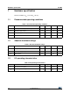
Table 7. Module pin usage
Pin Name Description Optional
1 TXRXLED
An active-low open drain output that can drive an external LED for
TX/RX activity status indication. TXRXLED must be enabled by setting
the value to 1 in register S24.
Yes
2 SHDN
Drive this signal low to put the module into a low power shutdown
mode. Drive the signal high to wake the module.
Yes
3 GPIO0 Reserved for future use, do not connect. Yes
4 GPIO1 Reserved for future use, do not connect. Yes
5MODE0
Drive this signal high to force the module into operating mode. Drive
this signal low to force the module into command mode. This enables
faster switching between modes and obviates the need for escape
sequences. After setting the MODE0 value, do a RESET to make the
new setting effective.
Yes
6 MODE1 Reserved for future use, do not connect. Yes
7 VDD Connect to power supply, 1.8V to 3.6V. No
8 GND Connect to system ground. No
9SWDIO
These signals are the serial wire debug (SWD) interface to the
STM32L microcontroller, supporting the development and loading of
custom firmware.
Yes
10 SWCLK Yes
11 BOOTMODE
Drive this signal high at power up or reset to start the boot loader and
allow device firmware update over the UART interface.
Yes
12 RESET
Drive this signal low to hold the module in reset. Drive this signal high
to release the module from reset.
Yes
13 TXD Connect to the host system UART RXD input. No
14 RXD Connect to the host system UART TXD output. No
15 GPIO2 Reserved for future use. Yes
16 GPIO3 Reserved for future use. Yes