K P 6 -FX 2 A P e n tiu m ® II P r o c e s s o r b a s e d m a in b o a r d TRADEMARK All products and company names are trademarks or registered trademarks of their respective holders. The specification is subject to change without notice.
Technical Support Services If you need additional information or help during installation or normal use of this product, contact your retailer. If your retailer can not help you may E-Mail us with any questions at the following address epox@epox.com. Record your serial number before installing your KP6-FX 2 mainboard.
User Notice No part of this product, including the product and software may be reproduced, transmitted, transcribed, stored in a retrieval system, or translated into any language in any form by any means with the express written permission of EPoX Computer Company (hereinafter referred to as EPoX) except documentation kept by the purchaser for backup purposes.
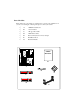
Parts Checklist Please make sure your package is complete before you start your installation. If you discover a damaged or missing item, please contact your retailer. √ √ √ √ √ √ √ A. B. C. D. E. F. G.
Table of Contents Page Introduction 1-1 1-1.1 1-1.2 1-2 1-3 1-3.1 1-3.2 1-4 Pentium® II Processor Overview --------------------------------------------- 1-1 S.E.C. Cartridge Overview ---------------------------------------------------- 1-2 S.E.C.
Table of Contents Appendixes Appendix Appendix Appendix Appendix Appendix Appendix A-1: A-2: A-3: A-4: A-5: B: Memory Map -------------------------------------------------- A1 I/O Map --------------------------------------------------------- A1 Time & DMA Channels Map ------------------------------- A2 Interrupt Map -------------------------------------------------- A2 RTC & CMOS RAM Map ----------------------------------- A3 Post Codes ------------------------------------------------------ B1
Introduction 1-1 Introduction EPoX is proud to introduce the KP6-FX 2 mainboard to support Intel Pentium® II Processor Intel’s latest technology in CPU’s. The KP6-FX 2 is based on Intel’s 82440FX chipset, and supports uni-Pentium® II Processor processor. Full specifications include 4 PCI and 4 ISA slots, USB ready, and a special ring-in feature all built into full ATX format. KP6-FX 2 also supports a memory capacity upto 1GB to run the most demanding applications.
KP6-FX 2 1-2 1-1.1 S.E.C. Cartridge Overview The entire enclosed product is called the Pentium® II Processor. The packaging technology and each of the physical elements of the product are referred to using accurate technical descriptions. This allows clear reference to the products as just a processor. This is the model used in past packaging technologies like PGA, TCP, PQFP, DIP, etc. 1-1.2 S.E.C.
Introduction 1-3 1-2 KP6-FX 2 Specification • • • • • • • • • • • • • • • • • • KP6-FX 2 is based on the Pentium® II Processor operating at 233 ~ 300 MHz on slot 1. The board is configured by an Easy-Setting-Single-Jumper (ESSJ) to match your CPU clock speed. Designed with Intel’s 82440 FX PCIset Supports upto 1 GigaByte of DRAM (minimum of 8 MB) on board, You can use either 72-Pin SIMM x 4 or 168-Pin DIMM x 2 or both.
KP6-FX 2 1-3 1-4 KP6-FX 2 Form-Factor Overview EPoX KP6-FX 2 is designed with ATX form factor - the latest industry standard of chassis. The ATX form factor is essentially a Baby-AT baseboard rotated 90 degrees within the chassis enclosure and a new mounting configuration for the power supply. With these changes the processor is relocated away from the expansion slots, allowing them all to hold full length add-in cards.
Introduction 1-3 1-5 I/O Shield Connector The KP6-FX 2 is equipped with an I/O back panel. Please use the appropriate I/ O shield. (refer to figure 1-3) Parallel Port Figure 1-3: KP6-FX 2 I/O back panel Layout PS/2 Mouse PS/2 Keyboard USB COM1 COM2 1-3.1 Power-On/Off (Remote) The KP6-FX 2 has a single 20-PIN connector for ATX power supplies. For ATX power supplies that support the Remote On/Off feature, this should be connected to the systems front panel for system Power On/Off button.
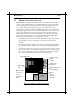
KP6-FX 2 1-6 1-4 System Block Diagram Pentium® II Processor Processor HOST BUS MAIN MEMORY PMC PCI Bridge and memory controller 208 PQFP MD[63:0] MA[11:0] > CONTROL > < > PD[15:0] < > > CONTROL PCI Slots DBX Data Bus Accelerator 208PQFP IDE CD-ROM PIIX3 PCI BUS I/O Bridge Port_A Port_B Graphics IDE HDD 208 PQFP Universal Serial Bus ISA Slots BIOS Flash Memory Figure 1-4 System Block Diagram SMC 37C932FR
Installation 2-1 Installation 2-1 KP6-FX 2 Layout The KP6-FX 2 is designed with Intel 82440FX PCIset chipset which is developed by Intel Corporation to fully support PCI/ISA systems. The Intel 82440FX PCIset chipset provides increased integration and improved performance. The chipset provides an integrated IDE controller with two high performance IDE interfaces for up to four IDE devices (hard drives, CD-ROM’s, etc.).
KP6-FX 2 2-2 KP6-FX 2 Layout PCI #5 Figure 2-1
Installation 2-2 2-3 Connectors and Jumpers This section describes all of the connectors and jumpers built into the motherboard. The jumpers match Figure 2-1 on page 2-2 J16 1 Power On/Off J9 + IDE LED indicator - LED ON when Onboard PCI IDE Hard disks activate + Power Saving LED indicator - LED ON when system is in any saving mode Sleep/Resume switch : Closed to enter sleep mode, a keystroke or mouse movement will instantly "wake up".
KP6-FX 2 2-2 2-4 Connectors and Jumpers (continued) Settings will match motherboard layout on Page 2-2 Clear CMOS Select 1-2 Normal (Default) 2-3 Clear 1 2 3 JP2 JP3 JP1 3 2 1 3 2 1 GND +12V GND JP6 JP5 6 5 4 3 2 1 Flash Memory Voltage Select (Both JP2 & JP3) 1-2 12V Flash memory 2-3 5V Flash memory. (Default) The Power Supply (+12V) for the CPU cooling fan. Memory Voltage Selection 1-2 & 4-5 Reserved 2-3 & 5-6 3.3V DIMM module (Default) 5 IrDA/ASK IR CONNECTOR: 1. VCC 2. FIRRX 3. IRRXX 4.
Installation 2-3 I/O Connectors J17 Floppy Disk Connector 34 2 33 2-5 J18,J19 Primary/Secondary IDE Connector 40 39 2 1 1 17
KP6-FX 2 2-3 2-6 I/O Connectors - continued 11 1 20 10 3.3 V -12 V GND PS-ON GND GND GND -5 V 5V 5V 11 12 13 14 15 16 17 18 19 20 1 2 3 4 5 6 7 8 9 10 3.3 V 3.3 V GND 5V GND 5V COM PW-OK 5 VSB 12 V Note: The ATX power supply has to support 3.
Installation 2-4 2-7 Memory Configurations The KP6-FX 2 supports different type of settings for the system memory. There is no jumper nor connector needed for memory configuration. The following figure provides all possible memory combinations. SIMM = 4MB, 8MB, 16MB, 32MB, 64MB, 128MB Fastpage or EDO mode SIMM DIMM = 8MB, 16MB, 32MB, 64MB, 128MB, 512MB Fastpage or EDO mode DIMM (3.3 volt unbuffered recommended) NOTE : 1.
KP6-FX 2 3-1 Award BIOS SETUP Award's ROM BIOS provides a built-in Setup program which allows user to modify the basic system configuration and hardware parameters. The modified data will be stored in a battery-backed CMOS so data will be retained even when the power is turned off. In general, the information saved in the CMOS RAM will stay unchanged unless there is a configuration change in the system, such as hard drive replacement or a device is added.
Award BIOS SETUP 3-2 3-1 STANDARD CMOS SETUP Choose "STANDARD CMOS SETUP" in the CMOS SETUP UTILITY Menu (Fig.3-2). The STANDARD CMOS SETUP allows user to configure system settings such as the current date and time, type of hard disk drive installed, floppy drive type, and display type. Memory size is auto-detected by the BIOS and displayed for your reference.
KP6-FX 2 3-3 Pressing [F1] key to display help message of the selected item. This provides the system a capability to recover from any possible error. ROM PCI/ISA BIOS BIOS FEATURES SETUP AWARD SOFTWARE, INC.
Award BIOS SETUP 3-4 • CPU Internal Cache / External Cache: These two categories increase • • performance to memory access. The Pentium® II Processor CPU includes both Internal/External cache. The default value is Enable. Note: If your Pentium® II Processor CPU is without External Cache then this item " External Cache" will not be shown. Enabled: Enable cache. Disable: Disable cache. Quick Power On Self Test: This category speeds up Power On Self Test (POST) after you power on the computer.
KP6-FX 2 3-5 • Gate A20 Option: This refers to the way the system addresses memory above 1MB (extended memory). The default value is Fast. Normal: The A20 signal is controlled by keyboard controller or chipset hardware. Fast: The A20 signal is controlled by Port 92 or chipset specific method. • Typematic Rate Setting: This determines the keystrokes repeat rate. Enabled: Enable typematic rate and typematic delay programming. Disabled: Disable typematic rate and typematic delay programming.
Award BIOS SETUP 3-6 Disabled: Video shadow is disabled. • C8000 - CBFFF Shadow : CC000 - CFFFF Shadow: D0000 - D3FFF Shadow: D4000 - D7FFF Shadow: D8000 - DBFFF Shadow: DC000 - DFFFF Shadow: These categories determine whether optional ROM will be copied to RAM by 16K byte or 32K byte per unit and the size depends on chipset. Enabled: Optional shadow is enabled. Disabled: Optional shadow is disabled.
KP6-FX 2 3-7 • DRAM Speed Selection: This value must correspond to the speed of the • • • • • DRAM installed in your system. DO NOT change the default setting of this field, as determined by the system board manufacturer for the installed DRAM. This value is access speed, so a lower value means a faster system. The default value is 60ns. 60ns: (Faster) Burst Wait State, for 60~70ns Fast Page Mode/EDO DRAM. 70ns: (Slower) Burst Wait State, for 70ns Fast Page Mode/EDO DRAM.
Award BIOS SETUP 3-8 • DRAM RAS Only Refresh: Permits queuing up to four DRAM refresh • • • • requests, so DRAM can refresh at optimal times. The default value is Disabled. Enabled: The DRAM Refresh type is RAS only. Disabled: The DRAM Refresh type is CAS before RAS. ECC Checking/Generation: The default value is Enabled. ECC: This field is enabled the optional DRAM Error Checking and Correction (ECC) with 72-bit Wide memory.
KP6-FX 2 3-9 • CPU-To-PCI Write Post: • • • • • Enabled: Writes from the CPU to the PCI bus are buffered, to compensate for the speed differences between the CPU and the PCI bus. Disabled: The writes are not buffered and the CPU must wait until the write is complete before starting another write cycle. CPU-To-PCI IDE Posting: Enabled: To post write cycles from the CPU to the PCI IDE interface. IDE accesses are posted in the CPU to PCI buffers, for cycle optimization.
Award BIOS SETUP 3-10 3-4 POWER MANAGEMENT SETUP Choose the "POWER MANAGEMENT SETUP" in the CMOS SETUP UTILITY to display the following screen. This menu allows the user to modify the power management parameters and IRQ signals. In general, these parameters should not be changed unless it's absolutely necessary. ROM PCI/ISA BIOS POWER MANAGEMENT SETUP AWARD SOFTWARE, INC.
KP6-FX 2 3-11 B. Time-out parameters: System Doze The "System Doze" mode timer starts to count when there is no "PM events" occurred. The valid time-out setting is from 1 minute up to 1 hour. System Standby The "Standby" mode timer starts to count when "System Doze" mode timer timed out and no "PM events" occurred. Valid range is from 1 minute up to 1 hour. System Suspend This function works only when the Pentium® Pro Processor is installed.
Award BIOS SETUP 3-12 Standby Mode When the system standby mode timer times-out, it will enter the standby mode and retain CPU at slow working speed. The screen will be blanked out. Suspend Mode When the system suspend timer times-out, the system will enter the suspend mode and the chipset will stop CPU clock immediately. The power consumption in Suspend Mode is lower than in standby mode. The screen is also blanked out. HDD Standby Mode When system stop reading or writing HDD, the timer starts to count.
KP6-FX 2 3-5 3-13 PNP/PCI CONFIGURATION The PNP/PCI configuration program is for the user to modify the PCI/ISA IRQ signals when various PCI/ISA cards are inserted in the PCI or ISA slots. WARNING: Conflicting IRQ’s may cause the system to not find certain devices. ROM PCI/ISA BIOS PNP/PCI CONFIGURATION AWARD SOFTWARE, INC.
Award BIOS SETUP 3-14 • Used MEM base addr and Used MEM Length: The default value is N/A. The Used MEM base addr (CB00, CC00, D000, D400, D800, DC00) and Used MEM Length (8K, 16K, 32K, 64K) were to support the some specific ISA Legacy cards with requested memory space below 1M address. Now with these two funtions, users canm define where the used memory address is located and its length of the legacy area that is used by the legacy device to avoid the memory space conflict.
KP6-FX 2 3-15 Note: If you do not use the Onboard IDE connector, then you will need set Onboard Primary PCI IDE: Disabled and Onboard Secondary PCI IDE: Disabled from CHIPSET FEATURES SETUP UTILITY. The Onboard PCI IDE cable should be equal to or less than 18 inches (45 cm.). • IDE HDD Block Mode: Select Enabled only if your hard drives support • • • • • • • block mode. Enabled: Enabled IDE HDD Block Mode. Provides higher HDD transfer rates. Disabled: Disable IDE HDD Block Mode.
Award BIOS SETUP 3-16 • Onboard FDC Controller: The default value is Enabled. • • • • Enabled: Enable the Onboard SMC CHIP's floppy drive interface controller. Disabled: Disable the Onboard SMC CHIP's floppy drive interface controller. Onboard Serial Port 1: This field allows the user to select the serial port. The default value is Auto. AUTO: Enable Onboard Serial port 1 and address is Auto adjusted COM1: Enable Onboard Serial port 1 and address is 3F8H/IRQ4.
KP6-FX 2 3-17 • ECP Mode USE DMA: This field allows the user to sellect DMA1 or DMA3 for the ECP mode. The default value is DMA3. DMA1: The filed selects the rounting of DMA1 for the ECP mode. DMA3: The filed selects the rounting of DMA3 for the ECP mode. 3-7 LOAD SETUP DEFAULTS The "LOAD SETUP DEFAULTS" function loads the system default data directly from ROM and initializes the associated hardware properly. This function will be necessary only when the system CMOS data is corrupted.
Award BIOS SETUP 2. If CMOS is corrupted or the option was used earlier and the user wish to change default password, the SETUP UTILITY will display a message and ask for a confirmation. Confirm Password: After pressing the [Enter] key (ROM password if the option was not used) or current password (user-defined password), the user can change the password and store new one in CMOS RAM. A maximum of 8 characters can be entered. 3.
KP6-FX 2 3-19 The maximum number of cylinders, head & sectors for NORMAL mode are. 1024, 16 & 63. no. Cylinder (1024) x no. Head ( 16) x no. Sector ( 63) x no. per sector ( 512) 528 Megabytes If user set his HDD to NORMAL mode, the maximum accessible HDD size will be 528 Megabytes even though its physical size may be greater than that! LBA (Logical Block Addressing) mode: A new HDD accessing method to overcome the 528 Megabyte bottleneck.
Award BIOS SETUP Maximum HDD size: no. Cylinder x no. Head x no. Sector x bytes per sector 3-20 (1024) ( 32) ( 63) ( 512) 1 GigaByte Note: To support LBA or LARGE mode of HDDs, there must be some software involved. All the software is located in the Award HDD Service Routine (1NT 13h). It may fail to access a HDD with LBA (LARGE) mode selected if you are running under a Operating System which replaces the whole 1NT 13h.
Appendix A1 Appendix A: A-1 MEMORY MAP Address Range [00000-7FFFF] [80000-9FBFF] [9FC00-9FFFF] [A0000-C7FFF] [C8000-DFFFF] [E0000-EEFFF] [EF000-EFFFF] [F0000-F7FFF] [F8000-FCFFF] [FD000-FDFFF] [FE000-FFFFF] A-2 Size 512K 127K 1K 160K 96K 60K 4K 32K 20K 4K 8K Description Conventional memory Extended Conventional memory Extended BIOS data area if PS/2 mouse is installed Available for Hi DOS memory Available for Hi DOS memory and adapter ROMs Available for UMB Video service routine for Monochrome & CGA
Appendix A-3 A2 TIME & DMA CHANNELS MAP TIME MAP: TIMER TIMER TIMER Channel 0 Channel 1 Channel 2 DMA CHANNELS: DMA Channel 0 DMA Channel 1 DMA Channel 2 DMA Channel 3 DMA Channel 4 DMA Channel 5 DMA Channel 6 DMA Channel 7 A-4 System timer interrupt. DRAM REFRESH request. SPEAKER tone generator. Available. Onboard ECP (Option). FLOPPY DISK (SMC CHIP). Onboard ECP (default). Cascade for DMA controller 1. Available. Available. Available INTERRUPT MAP NMI : Parity check error.
Appendix A-5 RTC & CMOS RAM MAP RTC & CMOS: 00 Seconds. 01 Second alarm. 02 Minutes. 03 Minutes alarm. 04 Hours. 05 Hours alarm. 06 Day of week. 07 Day of month. 08 Month. 09 Year. 0A Status register A. 0B Status register B. 0C Status register C. 0D Status register D. 0E Diagnostic status byte. 0F Shutdown byte. 10 FLOPPY DISK drive type byte. 11 Reserve. 12 HARD DISK type byte. 13 Reserve. 14 Equipment type. 15 Base memory low byte. 16 Base memory high byte. 17 Extension memory low byte.
Appendix B1 Appendix B: B POST CODES ISA POST codes are typically output to I/O port address 80h. POST(hex) DESCRIPTION 01-02 C0 03 Reserved. Turn off OEM specific cache, shadow. 1. Initialize EISA registers (EISA BIOS only). 2. Initialize all the standard devices with default values Standard devices includes. -DMA controller (8237). -Programmable Interrupt Controller (8259). -Programmable Interval Timer (8254). -RTC chip. Reserved 1. Keyboard Controller Self-Test. 2. Enable Keyboard Interface.
Appendix 0D 0E 0F 10 11 12-13 14 15 16 17 19 1A-1D 1E 1F-29 30 31 32 33-3B 3C 3D 3E B2 1. Program some of the Chipset's value according to Setup. (Early Setup Value Program) 2. Measure CPU speed for display & decide the system clock speed. 3. Video initialization including Monochrome, CGA, EGA/VGA. If no display device found, the speaker will beep. 1. Test video RAM. (If Monochrome display device found) 2. Show messages including. - Award Logo, Copyright string, BIOS Data code & Part No.
Appendix 3F-40 BF 41 42 43 45 44 45 46-4D 4E 4F 50 51 52 53 60 B3 Reserved. 1. Program the rest of the Chipset's value according to Setup. (Later Setup Value Program) 2. If auto-configuration is enabled, programm the chipset with pre-defined Values. Initialize floppy disk drive controller. Initialize Hard drive controller. If it is a PnP BIOS, initialize serial & parallel ports. Reserved. Initialize math coprocessor. Reserved. If there is any error detected (such as video, kb...
Appendix 61 B4 1. Try to turn on Level 2 cache. Note: If L2 cache is already turned on in POST 3D, this part will be skipped. 2. Set the boot up speed according to Setup setting. 3. Last chance for Chipset initialization. 4. Last chance for Power Management initialization. (Green BIOS only) 5. Show the system configuration table. 62 1. Setup daylight saving according to Setup value. 2. Program the NUM Lock, typematic rate & typematic speed according to Setup setting. 63 1.
NOTE : The "LOAD SETUP DEFAULTS" function loads the system default data directly from ROM and initializes the associated hardware properly. This function will be necessary when you accept this mainboard, or the system CMOS data is corrupted. ROM PCI/ISA BIOS CMOS SETUP UTILITY AWARD SOFTWARE, INC.