82430TX PCIset EP-5ATXA-M ISA PCI M a in B o a rd with Onboard PCI IDE and Super Multi-I/O. TRADEMARK All products and company names are trademarks or registered trademarks of their respective holders. The specification is subject to change without notice.
User Notice No part of this product, including the product and software may be reproduced, transmitted, transcribed, stored in a retrieval system, or translated into any language in any form by any means with the express written permission of EPoX Computer Company (hereinafter referred to as EPoX) except documentation kept by the purchaser for backup purposes.
Package Checklist Please make sure your package which should include all items listed below. If you find any item damaged or missing items, please contact your supplier.
Contents page Chapter 1 - Introduction ................................................... 1-1 System Block Diagram ............................................. 1-3 EP-5ATXA-M Layout .............................................. 1-4 Chapter 2 - Hardware Design ......................................... 2-1 2-1 2-2 2-3 2-4 2-5 2-6 Overview ..................................................................2-1 Connectors and Jumpers ............................................
Read me first 1. The "LOAD SETUP DEFAULTS" function loads the system default data directly from ROM and initializes the associated hardware properly. This function is necessary when you accept this mainboard, or the system CMOS data will corrupt. ROM PCI/ISA BIOS CMOS SETUP UTILITY AWARD SOFTWARE, INC.
Introduction 1-1 Chapter 1 Introduction The EP-5ATXA-M mainboard is a high performance system hardware based on Intel Pentium R processor and is equipped with four PCI slots, four standard ISA slots, a PnP Super I/O controller and two dual-port PCI-IDE connectors for the future expansion. The hardware dimension is an ATX form-factor that is 208mm x 305mm with a four-layer design technology. Specification Intel 82430TX PCIset chipset.
1-2 EP-5ATXA-M Software power-down when using Windows R95. Supports Resume by Alarm-Allows your system to turn on at a preselected time. Supports USDM(Unifed System Diagnostic Manager) to monitor system CPU Fan speed, chassis Fan Speed, CPU temperature, System temperature, CPU R Voltage and power Supply Voltage in Windows R 95 or NT 4.0. Supports YAMAHA YMF-715 Audio with 3D sound. Supports the system power LED lights when the system is powered on and blinks in sleep or suspend mode.
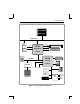
Introduction 1-3 R Pentium processor > > HOST BUS TAG > > PB SRAM MA[11:0] Control MTXC < < TAG Control HOST Bridge 324 BGA > > MD[63:0] > < CONTROL PCI Slots IDE CD-ROM PIIX4 PCI BUS I/O Bridge Port_A Port_B Graphics IDE HDD 324 BGA Universal Serial Bus Audio ISA Slots BIOS Flash EPROM Super I/O Figure 1-2 System Block Diagram Serial 1 Serial 2 FDD Printer
Hardware Design 2-1 Chapter 2 Hardware design 2-1 Overview The EP-5ATXA-M is designed with Intel 82430TX PCIset chipset which is developed by Intel Corporation to fully support Pentium ProcessorRPCI/ISA system. The Intel 82430TX PCIset chipset can increase integration and improve performance designs. The chipset provides an integrated IDE controller with two high performance IDE interfaces for up to four IDE devices (hard devices, CD-ROM device, etc).
2-2 EP-5ATXA-M The EP-5ATXA-M supports Award Plug & Play BIOS for the ISA and PCI cards. The BIOS can be located in Flash EPROM. The advantage of having Flash EPROM is much easier to replace BIOS code if necessary. The EP-5ATXA-M has been designed with ATX form-factor with ATX power connector. The mainboard layout and system block diagram are shown in Figure 1-1 and Figure 2-1.
Figure 2-1 1 2 1 RESET SPEAKER J6 JP1 JP3 J2 PCI#1 J9 Secondary IDE 1 5 PCI#3 1 3 26 25 KEYLOCK 10 G-LED J15 Primary IDE JP2 6 HD-LED MTXC 1 IR CONN SLEEP PCI#2 Power Conn. TB-LED J3 SOCKET 7 BANK0 BANK1 BANK2 PS/2 MOUSE K/B J4 J5 64K*64 SRAM M3 M2 M1 SIMM 2 SIMM 1 USB PORT ATX FDD CONN.
2-4 EP-5ATXA-M 2-2 Connectors and Jumpers This section describes all of the connectors and jumpers equipped in the mainboard. Please refer to Figure 2-1 for the location of each connector and jumper.The figure in the following means connecting pin 1&2 and means connecting pin 2&3. Jumpers with two pins are shown as for open and for close. JP3:CPU Clock Rate Select.
Hardware Design J4 1 2-5 KeyLock - Keyboard lock switch & Power LED connector. 1. Power LED(+) * The power LED lights when the system is powered on 2. N/C and blinks in SLEEP MODE 3. GND (Suspend mode). 4. Keylock 5. GND 5 Speaker - connect to the system's speaker for beeping. 7. Speaker 8. N/C 9. GND 10. VCC 7 10 Reset - Close to restart system. + Turbo LED indicator - LED ON when a higher speed is selected. + Harddisk LED indicator - LED ON when Onboard PCI IDE Harddisks activites.
2-6 EP-5ATXA-M JP1 1 3 JP13 1 Keyboard Power ON function: 1-2 : Enabled (For the details, please refer to Chapter 3-1: Keyboard Power On Function.) 2-3 : Disabled (Default) 3 1 J3 Clear CMOS: 1-2 : Normal operation (Default) 2-3 : Clear CMOS Values This setting allows users to clear current CMOS data and to return to the initial data by setting the jumper to 2-3 when the system is off. This jumper should be brought back to pin 1-2 to restore the normal operation.
Hardware Design 2-3 2-7 Real Time Clock Battery Replacement The battery can be replaced by a Sanyo / Panasonic CR2032, or other equivalent coin lithium battery. Please follow the steps below to replace the battery. 2.Insert 1.Remove + 1 + 1 2 + 2 3 4 + + 3 + + 2-4 System Memory Configuration The EP-5ATXA-M supports different types of settings for the system memory. There is not jumper for SDRAM hardware setting is for memory configuration.
2-8 EP-5ATXA-M SIMM2 SIMM1 > > > > DIMM3 DIMM2 DIMM1 BANK 2 BANK 2 BANK 1 BANK 0 5V FP / EDO DRAM 3.3V Synchronous DRAM or 3.3V FP/EDO DRAM 3.3V Synchronous DRAM or 3.3V FP/EDO DRAM 3.3V Synchronous DRAM or 3.3V FP/EDO DRAM MemoryConfigurationTable DIMM (M1) (BANK 0) DIMM2(M2) (BANK 1) SDRAM 8MB, 16MB SDRAM 8MB, 16MB x 1 32MB DIMM3(M3) (BANK 2) 32MB x 1 x 1 Empty Empty EDO/FP DRAM 4MB, 8MB x 2 = x 1 32MB = 32MB SDRAM 8MB, 16MB x 1 TOTAL Memery MAX.
Hardware Design 2-9 DIMM Module Installation Figure 2-2 displays the notch marks and what they should look like on your DIMM memory module. DIMMs have 168-pins and two notches that will match with the onboard DIMM socket. DIMM modules are installed by placing the chip firmly into the socket at a 90 degree angle and pressing straight down (figure 2-3) until it fits tightly into the DIMM socket (figure 2-4). LEFT KEY ZONE (UNBUFFERED) CENTER KEY ZONE (3.
2-10 EP-5ATXA-M When you have a DIMM module to plug into a 168-pin dual readout connnector, you must make sure that the DIMM module is 3.3V/Unbuffered to supports Intel PentiumRProcessor System. * EP-5ATXA-M Supports and extends many memory configurations on its 2 SIMM and 2 DIMM sites. The memory size of any configuration can be combined flexibly. BIOS will detect your memory configurations and sizes automaticallly. * The 70ns Fast Page Mode or 60ns EDO is necessary.
Hardware Design 2-11 2-6 Integrated PCI Bridge R The EP-5ATXA-M utilizes Intel 430TX PCIset chipset to support Intel Pentium Processor PCI/ISA system. The Intel 82430TX PCIset chipset consists of one 82439TX system controller (MTXC) and one 82371AB PCI ISA/IDE Accelerator (PIIX4) bridge chip. It provides an interface which translates CPU cycle into PCI bus cycle and PCI burst read/write capability.
Introduction 3-1 Chapter 3 ATX Form-Factor Overview The EP-5ATXA-M is base on ATX form-factor with a board size 8.2" x 12" (208mm x 305mm). The ATX from-factor is essentially an enlarged baby-AT basedboard rotated 90 degrees within an ATX chassis and uses ATX power supply. The changes make pentium R processor able to locate away from the expansion slots and all onboard I/Os able to hold full length add-on cards.
3-2 EP-5ATXA-M The EP-5ATXA-M is equipped with a standard I/O back pannel featuring a serial port, PS/2 mouse port, PS/2 keyboard port, parallel port, and secondary serial port (refer to Figure 3-2 ). Figure 3-2: EP-5ATXA-M I/O back panel Layout The EP-5ATXA-M supports ATX power connector which is a single 20-PIN input device for ATX power supply (see Figure 3-3).
Introduction 3-3 3-1 External Modem Ring-in Power ON and Keyboard Mouse Power ON Functions External Modem Ring-in Power-ON Function On the basis of bounded functions in I/O chipset, the two serial ports are able to support the External Modem Ring-in Power ON function. Once users connect the external modem to COM1 or COM2, the EP-5ATXA-M mainboard allows them to turn on their system through the remote and host's dial-up control.
AWARD BIOS 4-1 Chapter 4 Award BIOS Setup Award's ROM BIOS provides a built-in Setup program which allows user to modify the basic system configuration and hardware parameters. The modified data will be stored in a battery-backed CMOS RAM so data will be retained even when the power is turned off. In general, the information saved in the CMOS RAM stay unchanged unless there is a configuration change in the system, such as hard drive replacement or new equipment change.
4-2 CHAPTER 4 4-1 Standard CMOS Setup Choose "STANDARD CMOS SETUP" in the CMOS SETUP UTILITY Menu (Fig.4-1). The STANDARD CMOS SETUP allows user to configure system setting such as current date and time, type of hard disk drive installed in the system, floppy drive type, and the type of display monitor. Memory size is auto-detected by the BIOS and displayed for your reference.
AWARD BIOS 4-3 ROM PCI/ISA BIOS(2A59IPAB) BIOS FEATURES SETUP AWARD SOFTWARE, INC.
4-4 CHAPTER 4 Quick Power On Self Test:This category speeds up Power On Self Test (POST) after you power on the computer. If it is set to Enabled, BIOS will shorten or skip some check items during POST. The default is Enabled. Enabled : Enable quick POST. Disabled: Normal POST. Boot Sequence:This category determines which drive is searched first for the O/S (Operating System). Default value is A, C, SCSI. The following is your list of options.
AWARD BIOS 4-5 Gate A20 Option: This refers to the way the system addresses memory above 1MB (extended memory). The default value is Fast. Normal : The A20 signal is controlled by keyboard controller or chipset hardware. Fast : The A20 signal is controlled by Port 92 or chipset specific method. Typematic Rate Setting: This determines the keystroke repeat rate. Enabled : Enable typematic rate and typematic delay programming. Disabled: Disable typematic rate and typematic delay programming.
4-6 CHAPTER 4 C8000 - CBFFF Shadow : CC000 - CFFFF Shadow: D0000 - D3FFF Shadow: D4000 - D7FFF Shadow: D8000 - DBFFF Shadow: DC000 - DFFFF Shadow: These categories determine whether other expansion card optional ROM will be copied to RAM by 16K byte or 32K byte per unit and the size depends on chipset. If you install other expansion cards with ROMs on them, you will need to know which addresses the ROMs use to shadow themselves specifically. Enabled : Optional shadow is enabled.
AWARD BIOS 4-7 Note: When you insert slow memory modules in the system and set a faster timing, the system may hang up. DRAM Timing: The default value is 60ns. 60ns : 2 (faster) Burst Wait State, for 60~70ns Fast Page Mode/EDO DRAM. 70ns : 3 (slower) Burst Wait State, for 70ns Fast Page Mode/EDO DRAM. DRAM Leadoff Timing: The default value is 10/6/3 (Read Leadoff / Write Leadoff / RAS# Precharge) 10/6/3 : For EDO / FPM reads and Writes timing. 11/7/3 : For slow EDO /FPM reads and Writes timing.
4-8 CHAPTER 4 Video BIOS Cacheable: The default value is enabled. Enabled : This field Enables the Video BIOS Cacheable to speed up the VGA Performance. Disabled: Disables the Video BIOS Cacheable function. 8/16 Bit I/O Recovery Time: The default value is 1. 8 Bit I/O Recovery Time: This field defines the recovery time from 1 to 8 for 8bit I/O. 16 Bit I/O Recovery Time: To define the recovery time from 1 to 4 for 16-bit I/O. Memory Hole at 15M-16M: The default value is disabled. Disabled: Normal Setting.
AWARD BIOS 4-9 4-4 Power Management Setup Choose the "POWER MANAGEMENT SETUP" in the CMOS SETUP UTILITY to display the following screen. This menu allows users to modify the power management parameters and IRQ signals. In general, these parameters should not be changed unless it is absolutely necessary. ROM PCI/ISA BIOS (2A59IPAB) POWER MANAGEMENT SETUP AWARD SOFTWARE, INC.
4-10 CHAPTER 4 B. Time-out parameters : HDD Standby The HDD Standby timer can be set from 1 to 15 minute(s). System Doze The "System Doze" mode timer starts to count when no "PM event" occurres. The valid time-out setting is from 1 minute up to 1 hour. System Standby The "Standby" mode timer starts to count when the "System Doze" mode timer times out and no "PM events" occurre. The valid range is from 1 minute up to 1 hour. System Suspend R This function works only when the Pentium Procssor is installed.
AWARD BIOS 4-11 MODEM Use IRQ: Name the interrupt request (IRQ) line assigned to the modem (if any) on your system. Activity of the selected IRQ always awakens the system. Default is IRQ 3. N/A: No IRQ is used. 4: IRQ 4 7: IRQ 7 10: IRQ 10 3: IRQ 3 5: IRQ 5 9: IRQ 9 11: IRQ 11 The KP6-LA supports HDD Power Down, Doze and Standby power saving functions when using the Intel Pentium II Processor. The default is Disabled Doze Mode: The "Doze" mode timer starts to count when no "PM events" have occurred.
4-12 CHAPTER 4 Resume by Ring: This option is used to set the remote ring in feature. The default is Enabled. Enabled: The system can use remote ring-in to wake the system up. Disabled: The system cannot use remote ring in to wake system up. Power Loss Recovery: If the power to the system is cut off the system will turn itself back on with no user intervention. The default is Enabled. Enabled: The system will power back on after a power interuption.
AWARD BIOS 4-13 The EP-5ATXA-M supports HDD Power Down, Doze and standby power savingfunctions when Intel Pentium RProcessor is installed. In addition, the suspend function is supported when the JP14's sleep (sleep ref. Figure1-1) is closed to enter the green function. The detailed descriptions of these functions are provided in the next page. HDD Power Down When the system stops reading or wiriting HDD, the timer starts to count. The system will cut off the HDD power when timer runs out of time.
4-14 CHAPTER 4 ROM PCI/ISA BIOS(2A59CPA9) PNP/PCI CONFIGURATION AWARD SOFTWARE, INC.
AWARD BIOS 4-15 Used MEM base addr and Used MEM Length : The default value is N/A. The Used MEM base addr (CB00, CC00, D000, D400, D800, DC00) and Used MEM Length (8K, 16K, 32K, 64K) support some specific ISA Legacy cards with requested memory space below 1M address. Now with these two functions, users can define where the used memory address is located and its length of the legacy area corresponding.
4-16 CHAPTER 4 4-6 Integrated Peripherals ROM PCI/ISA BIOS(2A59IPAB) INTEGRATED PERIPHERALS WARD SOFTWARE, INC.
AWARD BIOS 4-17 IDE Primary Master PIO: The default value is Auto. Auto : BIOS will automatically detect the Onboard Primary Master PCI IDE HDD Accessing mode. Mode0~4 : Manually set the IDE Accessing mode. IDE Primary Slave PIO: The default value is Auto. Auto : BIOS will automatically detect the Onboard Primary Slave PCI IDE HDD Accessing mode. Mode0~4 : Manually set the IDE Accessing mode. IDE Secondary Master PIO: The default value is Auto.
4-18 CHAPTER 4 Onboard UART 2 Mode:The default value is standard. This field allows the user to select the COM2 port that can support a serial Infrared Interface. Standard:Support a Serial Infrared Interface IrDA. HPSIR:Support a HP Serial Infrared Interface formats. ASKIR:Support a Sharp Serial Infrared Interface formats. Onboard Parallel port: This field allows the user to sellect the LPT port. The default value is 378H/IRQ7.
AWARD BIOS 4-19 ROM PCI/ISA BIOS(2A59IPAB) CMOSSETUPUTILITY AWARD SOFTWARE, INC.
4-20 CHAPTER 4 4-9 IDE HDD Auto Detection The "IDE HDD AUTO DETECTION" utility is a very useful tool especially when you do not know which kind of hard disk type you are using. You can use this utility to detect the correct disk type installed in the system automatically. But now you can set HARD DISK TYPE to Auto in the STANDARD CMOS SETUP. You don't need the "IDE HDD AUTO DETECTION" utility. The BIOS will Auto-detect the hard disk size and model on display during POST.
AWARD BIOS 4-21 LBA (Logical Block Addressing) mode: A new HDD accessing method to overcome the 528 Megabyte bottleneck. The numbers of cylinders, heads and sectors shown in the setup may not be the numbers physically contained in the HDD. During HDD accessing, the IDE controller will transform the logical address described by sector, head and cylinder into its own physical address inside the HDD. The maximum HDD size supported by LBA mode is 8.4 Gigabytes which is obtained from the following formula: no.
4-22 CHAPTER 4 Note: To support LBA or LARGE mode of HDDs, there must be some softwares involved. All these softwares are located in the Award HDD Service Routine (1NT 13h). It may be failed to access a HDD with LBA (LARGE) mode selected if you are running under an Operating System which replaces the whole 1NT 13h. UNIX operating systems do not support either LBA or LARGE and must utilize the Standard mode. However UNIX can support drives larger than 528MB.
TECHNICAL INFORMATION 5-1 Chapter 5 Technical Information 5-1 I/O & MEMORY MAP MEMORY MAP Address Range [00000-7FFFF] [80000-9FBFF] [9FC00-9FFFF] [A0000-C7FFF] [C8000-DFFFF] [E0000-EEFFF] [EF000-EFFFF] [F0000-F7FFF] [F8000-FCFFF] [FD000-FDFFF] [FE000-FFFFF] Size 512K 127K 1K 160K 96K 60K 4K 32K 20K 4K 8K Description Conventional memory Extended Conventional memory Extended BIOS data area if PS/2 mouse is installed Available for Hi DOS memory Available for Hi DOS memory and adapter ROMs Available for UMB
5-2 CHAPTER 5 5-2 Time & DMA Channels Map TIME MAP: TIMER Channel 0 TIMER Channel 1 TIMER Channel 2 System timer interrupt. DRAM REFRESH request. SPEAKER tone generator. DMA CHANNELS : DMA Channel 0 DMA Channel 1 DMA Channel 2 DMA Channel 3 DMA Channel 4 DMA Channel 5 DMA Channel 6 DMA Channel 7 Available. Onboard ECP (Option). FLOPPY DISK (SMC CHIP). Onboard ECP (default). Cascade for DMA controller 1. Available. Available. Available. 5-3 Interrupt Map NMI : IRQ (H/W) : Parity check error.
TECHNICAL INFORMATION 5-3 5-4 RTC & CMOS RAM Map RTC & CMOS : 00 01 02 03 04 05 06 07 08 09 0A 0B 0C 0D 0E 0F 10 11 12 13 14 15 16 17 18 19-2d 2E-2F 30 31 32 33 35-3F 40-7F Seconds. Second alarm. Minutes. Minutes alarm. Hours. Hours alarm. Day of week. Day of month. Month. Year. Status register A. Status register B. Status register C. Status register D. Diagnostic status byte. Shutdown byte. FLOPPY DISK drive type byte. Reserve. HARD DISK type byte. Reserve. Equipment type. Base memory low byte.
5-4 CHAPTER 5 Appendix A: POST Codes ISA POST codes are typically output to port address 80h. POST(hex) DESCRIPTION 01-02 Reserved. C0 Turn off OEM specific cache, shadow. 03 1.Initialize EISA registers (EISA BIOS only). 2.Initialize all the standard devices with default values Standard devices includes. -DMA controller (8237). -Programmable Interrupt Controller (8259). -Programmable Internal Timer (8254). -RTC chip. 04 Reserved 05 1.Keyboard Controller Self-Test. 2.Enable Keyboard Interface.
TECHNICAL INFORMATION 5-5 POST(hex) DESCRIPTION 0C Initialization of the BIOS Data Area. (40:ON - 40:FF) 0D 1.Program some of the Chipset's value according to Setup (Early Setup Value Program). 2.Measure CPU speed for display and decide the system clock speed. 3.Video initialization including Monochromc, CGA and EGA/VGA. If no display device found, the speaker will beep up. 0E 1.Test video RAM (If Monochromc display device found). 2.
5-6 CHAPTER 5 POST(hex) DESCRIPTION 32 1.Display the Award Plug & Play BIOS Extension message (PnP BIOS only). 2.Program all onboard super I/O chips (if any) including COM ports, LPT ports, FDD port ... according to setup value. 33-3B Reserved. 3C Set flag to allow users to enter CMOS Setup Utility. 3D 1.Initialize Keyboard. 2.Install PS/2 mouse. 3E Try to turn on Level 2 cache. Note : Some chipset may need to turn on the L2 cache in this stage. But usually, the cache is turn on later in POST 61h.
TECHNICAL INFORMATION 5-7 POST(hex) DESCRIPTION 52 1.Initialize all ISA ROMs. 2.Later PCI initializations (PCI BIOS only). -Assign IRQ to PCI devices. -Initialize all PCI ROMs. 3.PnP Initialzations. (PnP BIOS only) -Assign IO, Memory, IRQ & DMA to PnP ISA devices. -Initialize all PnP ISA ROMs. 4.Program shadows RAM according to Setup settings. 5.Program parity according to Setup setting. 6.Power Management Initialization. -Enable/Disable global PM. -APM interface initialization. 53 1.
5-8 CHAPTER 5 Appendix B: I/O Connectors JP13 : PS/2 Mouse Connector: Pin 1 2 3 4 5 Signal Name Data Clock GND NC VCC (Red Wire) (Blue Wire) (Green Wire) (Yellow Wire) JP10/COM1, JP11/COM2 : Serial Ports Connector Signal Name 6 9 1 5 DCD SIN SOUT DTR GND Pin Pin Signal Name 1 2 3 4 5 6 7 8 9 DSR RTS CTS RI Signal Name Pin Pin Signal Name STROBEData Bit 0 Data Bit 1 Data Bit 2 Data Bit 3 Data Bit 4 Data Bit 5 Data Bit 6 Data Bit 7 ACJBUSY PE SLCT 1 2 3 4 5 6 7 8 9 10 11 12 13 14 15 16 17
TECHNICAL INFORMATION 5-9 J7 : Floppy Disk Connector Signal Name 1 2 33 34 Ground Ground Ground Ground Ground Ground Ground Ground Ground Ground Ground Ground Ground Ground Ground Ground Ground Pin 1 3 5 7 9 11 13 15 17 19 21 23 25 27 29 31 33 Pin 2 4 6 8 10 12 14 16 18 20 22 24 26 28 30 32 34 Signal Name FDHDIN Reserved FDEDIN IndexMotor Enable Drive Select BDrive Select AMotor Enable DIRSTEPWrite Data Write Gate Track 00Write ProtectRead DataSIDE 1 SELECTDiskette J5/J6 : Primary, Secondray IDE C
5-10 CHAPTER 5 ATX Power Supply Connector: Signal Name 11 20 1 10 Pin Pin 3.3V 11 1 3.3V -12.0V 12 2 3.3V GND 13 3 GND PS-ON 14 4 5.0V GND 15 5 GND GND 16 6 5.0V GND 17 7 GND -5.0V 18 8 PW-OK 5.0V 19 9 5VSB 5.0V 20 10 12.