S1D13513 Display Controller S5U13513P00C100 Evaluation Board User Manual Document Number: X78A-G-003-01 Status: Revision 1.0 Issue Date: 2007/03/30 © SEIKO EPSON CORPORATION 2006-2007. All Rights Reserved. Information in this document is subject to change without notice. You may download and use this document, but only for your own use in evaluating Seiko Epson/EPSON products. You may not modify the document. Epson Research and Development, Inc.
Page 2 Epson Research and Development Vancouver Design Center S1D13513 X78A-G-003-01 S5U13513P00C100 Evaluation Board User Manual Issue Date: 2007/03/30 Revision 1.
Epson Research and Development Vancouver Design Center Page 3 Table of Contents 1 Introduction . . . . . . . . . . . . . . . . . . . . . . . . . . . . . . . . . . . . . . . . 5 2 Features . . . . . . . . . . . . . . . . . . . . . . . . . . . . . . . . . . . . . . . . . . 6 3 Installation and Configuration . . . . . . . . . . . . . . . . . . . . . . . . . . . . . . 7 3.1 Configuration DIP Switch . . . . . . . . . . . . . . . . . . . . . . . . . . . 7 3.2 Configuration Jumpers . . . . . . . . . . . . .
Page 4 Epson Research and Development Vancouver Design Center S1D13513 X78A-G-003-01 S5U13513P00C100 Evaluation Board User Manual Issue Date: 2007/03/30 Revision 1.
Epson Research and Development Vancouver Design Center Page 5 1 Introduction This manual describes the setup and operation of the S5U13513P00C100 Evaluation Board. The evaluation board is designed as an evaluation platform for the S1D13513 Display Controller. The S5U13513P00C100 evaluation board can connect to the S5U13U00P00C100 USB Adapter board so that it can be used with a laptop or desktop computer, via USB 2.0.
Page 6 Epson Research and Development Vancouver Design Center 2 Features The S5U13513P00C100 Evaluation Board includes the following features: • 256-pin PBGA S1D13513 Display Controller • On-board SDRAM, selectable as 8MB x 32-bit or 8MB x 16-bit • Headers for connection to the S5U13U00P00C100 USB Adapter board or to the PC Card Extender board • Headers for connecting to various Host Bus Interfaces • Headers for connecting to LCD panels • Headers for connecting to cameras • On-board 10MHz crystal (used fo
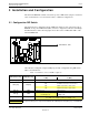
Epson Research and Development Vancouver Design Center Page 7 3 Installation and Configuration The S5U13513P00C100 evaluation board incorporates a DIP switch, jumpers, and 0 ohm resistors which allow it to be used with a variety of different configurations. 3.1 Configuration DIP Switch The S1D13513 has configuration inputs (CNF[8:0]) which are read on the rising edge of RESET#. A 10-position DIP switch (SW1) is used to configure the S1D13513 for multiple Host Bus Interfaces.
Page 8 Epson Research and Development Vancouver Design Center Table 3-2: CNF[4:0] Setting for CNF[6] = 1b CNF[4:0] Host Bus 00000b Parallel Direct 80 Type 2: 1 CS# 00001b Parallel Direct 80 Type 3: 1 CS# 00010b Parallel Indirect 80 Type 2 00011b Parallel Indirect 80 Type 3 00100b Parallel Direct 80 Type 1: 1 CS# 00101b Parallel Direct 68: 1 CS# 00110b Parallel Indirect 80 Type 1 00111b Parallel Indirect 68 01000b Parallel Direct 80 Type 2: 2 CS# 01001b Parallel Direct 80 Type 3: 2 CS#
Epson Research and Development Vancouver Design Center Page 9 Table 3-3: CNF[4:0] Setting for CNF[6] = 0b CNF[4:0] Host Bus 00000b Generic Little Endian: Active Low WAIT# with tri-state 00001b Generic Little Endian: Active Low WAIT# always driven 00010b Generic Little Endian: Active HIgh WAIT# with tri-state 00011b Reserved 00100b Generic Big Endian: Active Low WAIT# with tri-state 00101b Generic Big Endian: Active Low WAIT# always driven 00110b Generic Big Endian: Active HIgh WAIT# with tr
Page 10 Epson Research and Development Vancouver Design Center 3.2 Configuration Jumpers The S5U13513P00C100 has 11 jumper blocks which configure various board settings. The jumper positions for each function are shown below.
Epson Research and Development Vancouver Design Center Page 11 JP1-JP10 - Power Supplies for the S1D13513 JP1-JP10 can be used to measure current consumption of each S1D13513 power supply. When the jumper is at position 1-2, normal operation is selected. When no jumper is installed, the current consumption for each power supply can be measured by connecting an ammeter to pin 1 and 2 of the jumper.
Page 12 Epson Research and Development Vancouver Design Center JP11 - SDRAM Width Select JP11 is used to select the bus width of the external SDRAM. When the jumper is at position 1-2, the external SDRAM is 32-bit wide and memory size is 32MB. The memory consists of 2 chips in parallel, each 16MB and 16-bit wide. When the jumper is at position 2-3, the external SDRAM is 16-bit wide and memory size is 16MB. In this position one memory chip is disabled and only one chip is active (16MB and 16-bit wide).
Epson Research and Development Vancouver Design Center Page 13 4 Technical Description 4.1 Power 4.1.1 Power Requirements The S5U13513P00C100 evaluation board requires an external regulated power supply (3.3V at 1A). The power is supplied to the evaluation board through pin 5 of the P2 header, or pin 29 of the H2 header. The green LED ‘3.3V Power’ is turned on when 3.3V power is applied to the board. 4.1.
Page 14 Epson Research and Development Vancouver Design Center CIOVDD1 is connected to 3.3V through a 0 ohm resistor, R70. If it is desired to have a different voltage for CIOVDD1, R70 must be removed and the desired supply connected to pin 15 of connector H6. HVDD5 is always connected to 3.3V. Note The recommended range for HVDD1 (HIOVDD), HVDD2 (PIOVDD), HVDD3 CIOVDD2), and HVDD4 (CIOVDD1) is 3.0V~3.6V. 4.2 Clocks S1D13513 has four clock inputs: BUSCLK, OSC1, OSC2 and CLKI3.
Epson Research and Development Vancouver Design Center Page 15 4.4 Host Interface 4.4.1 Connecting to the Epson S5U13U00P00C100 USB Adapter Board The S5U13513P00C100 evaluation board is designed to connect to a S5U13U00P00C100 USB Adapter Board. The USB adapter board provides a simple connection to any computer via a USB 2.0 connection. The S5U13513P00C100 directly connects to the adapter board through connectors P1 and P2. The USB adapter board also supplies the 3.
Page 16 Epson Research and Development Vancouver Design Center 4.4.3 Direct Host Bus Interface Support The S1D13513 Display Controller directly supports many host bus interfaces. For detailed S1D13513 pin mapping, refer to the S1D13513 Hardware Functional Specification, document number X78B-A-001-xx. All S1D13513 host interface pins are available on connectors H2 and H3 which allow the S5U13513P00C100 to be connected to a variety of development platforms.
Epson Research and Development Vancouver Design Center Page 17 4.5 LCD Panel Interface The LCD interface signals are available on connectors H4 and H5. Connector H5 includes GPIOG[4:0] which may be used as additional signals for extended TFT interfaces. For S1D13513 LCD interface pin mapping, refer to the S1D13513 Hardware Functional Specification, document number X78B-A-001-xx. Connectors H4 and H5 are both 0.1x0.1” 40-pin headers (20x2).
Page 18 Epson Research and Development Vancouver Design Center 4.6 Camera Interface All the signals for the Camera1 interface are available on connector H6. All the signals for the Camera2 interface are available on connector H7. H6 and H7 are 0.1x0.1” 20-pin headers (10x2). For the pinout of connectors H6 and H7, see “Schematic Diagrams” on page 24. The S1D13513 Camera1 interface signals use the GPIOC[7:0] and GPIOD[3:0] pins. The Camera2 interface signals use the GPIOA[7:0] and GPIOB[7:0] pins.
Epson Research and Development Vancouver Design Center Page 19 4.7 YUV Output for TV Display The S1D13513 can output YUV data which can be used to display an image on a TV screen via an external video encoder. The YUV output is multiplexed with other functions on the GPIOC[7:0] and GPIOD[2:0] pins. These pins are routed to connector H6. 4.8 Keypad Interface The S1D13513 has a 5x5 keypad interface which is multiplexed with other functions on the GPIOA[4:0] and GPIOB[4:0] pins.
Page 20 Epson Research and Development Vancouver Design Center 4.11 JTAG Connector The S1D13513 design includes a JTAG interface. All the JTAG signals are available on connector H1, however, connector H1 is not populated on the board. For the pinout of connector H1, see “Schematic Diagrams” on page 24. The following diagram shows the location of the JTAG connector (H1).
Epson Research and Development Vancouver Design Center Page 21 5 Parts List Table 5-1: Parts List Item Reference Part 49 C1, C2, C3, C4, C5, C6, C7, C8, C9, C19, C22, C26, C28, C29, C30, C31, C32, C33, C34, C35, C43, C44, C45, C46, C47, C48, C49, C50, C51, C65, C66, C69, C70, C71, C72, C73, C74, C75, C76, C77, C78, C79, C80, C81, C82, C98, C100, C104, C105 0.
Page 22 Epson Research and Development Vancouver Design Center Table 5-1: Parts List Description Manufacturer / Part No. / Assembly Instructions Item Qty Reference Part 19 2 H6, H7 HEADER_10X2 20 10 JP1, JP2, JP3, JP4, JP5, JP6, JP7, JP8, JP9, JP10 21 1 JP11 HEADER 3 CONN HEADER VERT 3POS .
Epson Research and Development Vancouver Design Center Page 23 Table 5-1: Parts List Qty Reference Part 39 1 SW1 SW DIP-10 40 1 SW2 SW TACT-SPST SWITCH TACT SILVER PLT GULLWING ITT Industries KSC241GLFS 41 4 TPGND1, TPGND2, TPGND3, TP3.3VDD1 TP_SMT PC TEST POINT MINIATURE SMT Keystone 5015 42 0 T1 TP SIP 43 1 U1 S1D13513 PBGA256 44 2 U2, U3 IS42S16800D-7TL alternate Micron MT48LC8M16A2P-7E ISSI IS42S16800D-7TL 45 1 U4 TPS3801L30DCKR IC 2.
A B C D 3 3 DB[15:0] AB[20:0] CS# M/R# RD# RD/WR# WE0# WE1# WAIT# BS# BURST# BDIP# INT1# INT2# RESET# CLKI3 BUSCLK OSCI1 OSCO1 OSCI2 OSCO2 GPIOA0 GPIOA1 GPIOA2 GPIOA3 GPIOA4 GPIOA5 GPIOA6 GPIOA7 GPIOB0 GPIOB1 GPIOB2 GPIOB3 GPIOB4 GPIOB5 GPIOB6 GPIOB7 GPIOC0 GPIOC1 GPIOC2 GPIOC3 GPIOC4 GPIOC5 GPIOC6 GPIOC7 GPIOD0 GPIOD1 GPIOD2 GPIOD3 GPIOG0 GPIOG1 GPIOG2 GPIOG3 GPIOG4 3 3 3 3 3 2 2 3 2 2 2 2 4 4 4 4 4 4 4 4 4 4 4 4 4 4 4 4 4 4 4 4 4 4 4 4 4 4 4 4 4 4 4 4 4 N1 R1 L15 L9 P9 R9 T9
Revision 1.0 A 3.
A B C 5 R107 R108 3.3VDD TP3.
A B C D R96 3.3VDD 0 1 5 C101 1 1 1 1 1 1 1 1 1 4.
Page 28 Epson Research and Development Vancouver Design Center 7 S5U13513P00C100 Board Layout Figure 7-1: S5U13513P00C100 Board Layout - Top View S1D13513 X78A-G-003-01 S5U13513P00C100 Evaluation Board User Manual Issue Date: 2007/03/30 Revision 1.
Epson Research and Development Vancouver Design Center Page 29 Figure 7-2: S5U13513P00C100 Board Layout - Bottom View S5U13513P00C100 Evaluation Board User Manual Issue Date: 2007/03/30 S1D13513 X78A-G-003-01 Revision 1.
Page 30 Epson Research and Development Vancouver Design Center 8 References 8.1 Documents • Epson Research and Development, Inc., S1D13513 Hardware Functional Specification, document number X78B-A-001-xx. 8.2 Document Sources • Epson Research and Development Website: http://www.erd.epson.com. S1D13513 X78A-G-003-01 S5U13513P00C100 Evaluation Board User Manual Issue Date: 2007/03/30 Revision 1.
Epson Research and Development Vancouver Design Center Page 31 9 Technical Support 9.1 EPSON Display Controllers (S1D13513) Japan Seiko Epson Corporation IC International Sales Group 421-8, Hino, Hino-shi Tokyo 191-8501, Japan Tel: 042-587-5812 Fax: 042-587-5564 http://www.epson.co.jp/ North America Epson Electronics America, Inc. 2580 Orchard Parkway San Jose, CA 95131, USA Tel: (408) 922-0200 Fax: (408) 922-0238 http://www.eea.epson.com/ Taiwan Epson Taiwan Technology & Trading Ltd. 14F, No.
Page 32 Epson Research and Development Vancouver Design Center Change Record X78A-G-003-01 Revision 1.0 - Issued: March 30, 2007 • minor edits • updated schematics • updated parts list • added board layout X78A-G-003-00 Revision 0.02 • revised manual due to design changes • added new schematics • added new parts list X78A-G-003-00 Revision 0.01 • Initial draft of manual S1D13513 X78A-G-003-01 S5U13513P00C100 Evaluation Board User Manual Issue Date: 2007/03/30 Revision 1.