
Service manual


Operating Principles
Dl%Y4iOOO+
Service Manual
The +35
VDC
regulator circuit includes the following:
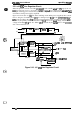
D
Input voltage line over-current protection arcuit (primary side)
IC101 and
IC201
detect the input voltage of the primary circuit. When the input voltage is normal,
the current does not flow into the shunt regulator. When the over-current flows to the input
voltage line, the shunt regulator is turned on,
Q103
(Q203)
and
Q102
(Q202)
are turned on, and
Q101
(Q201)
is turned off.
Q
+35
VDC
line over-current protection circuit
If the +35
VDC
line drops to +13
VDC,
the sensor circuit consisting of
R172
(R272)
and
R173
(R273)
turns on
Q153
(Q253).
Q154
is turned on, PC2 is turned on, and then the input voltage is cut. At this
time, the delay timing creation circuit (CR circuit) consisting of
C157 and
R174
makes the delay
timing.
When the printer is turned on, the delay timing creation circuit cannot start this protection
circuit; if it is operated during the
printhead
driver check, the power supply board cannot be
turned on. The CR circuit has approximately a one-second delay timing.
Cl
+35
VDC
powerdown detection circuit
When the +35
VDC
line drops (such as, when the printer has exceeded its duty cycle and the
printhead
temperature is too high), the voltage of PC101 approaches O
VDC.
If the voltage drops to
1.3
VDC,
IC152
outputs a HIGH
CLIMIT
signal to the base of transistor
Q187.
IC152
monitors the
two +35
VDC
line creation circuits.
Cl
+13
VDC
creation circuit
When the printer is turned on, the
C117
power supply board assembly creates +13
VDC
to check
the
printhead
drivers on the
C117
MAIN board assembly. After 140 ms, the
C117
MAIN board
assembly sends the
DRERR
(driver error) or the VPC (+35
VDC
permission) signal to the C117
power supply board assembly. If the
printhead
drivers are normal, the VPC signal is HIGH,
Q182
is turned on, and Q181 is turned off. Therefore, six
Zener
diodes create the +35
VDC.
During the
motor driver check, the VPC signal is LOW. When this signal is LOW, Q182 stays off, the base of
Q182
stays HIGH, and then two Zener diodes
(ZD151
and
ZD181)
output +13
VDC.
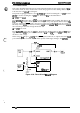
2.2.4
+/-12
VDC
Half-wave Rectifier Smoothing Circuit
The power from the half-wave rectifier smoothing circuit is mainly supplied to the RS-232C
interface on the standard or optional board and uses the
printhead
fire trigger. Both the
+12
VDC
and -12
VDC
lines have a half-wave rectifier circuit. This smoothing circuit consists of capacitors
C182
and
C181.
Two Zener diodes stabilize the *12
VDC
line.
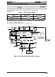
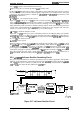
o
FMer
Circuit
surge-cut
Rectifier Smoothing
Circuit Circuit
C+
Icuit
o
I
I
J
4
)
TF
I
–
:
==
❑
“
~
-12VDC
Cteation
Main switching
Smoothing Circuit
(C181,182)
+
=
ci!:~=l~)
Smoothing Circuit
Circuit (1)
o
+
(C1SA3,161)
DerM3dvoltage
Conttd
arcut
o
+12VDC
Creation
Circut
+
Over Current
Protection
Transfmxmer
ZD187,1SS
(QIS3,184)
Cimuif
(ICI01,201)
+12
VDC
-12
WC
Figure 2-17. Half-wave Rectifier Circuit
2-16
Rev.
A