init ETX-945 User Manual High-Performance ETX 3.0 Compliant Computer-on-Modules Revision 1.00 Date Comment Initial Release FOR TECHNICAL SUPPORT PLEASE CONTACT: support@diamondsystems.com Copyright 2009 Diamond Systems Corporation 1255 Terra Bella Ave. Mountain View, CA 94043 USA Tel 1-650-810-2500 Fax 1-650-810-2525 www.diamondsystems.
CONTENTS IMPORTANT SAFE-HANDLING INFORMATION ......................................................................................................3 1. INTRODUCTION .................................................................................................................................................4 1.1 Features .........................................................................................................................................................4 1.2 ETX-945 Models .............
IMPORTANT SAFE-HANDLING INFORMATION WARNING: ESD-Sensitive Electronic Equipment! Observe ESD-safe handling procedures when working with this product. Always use this product in a properly grounded work area and wear appropriate ESD-preventive clothing and/or accessories. Always store this product in ESD-protective packaging when not in use. Safe Handling Precautions The ETX-945 contains numerous I/O connectors that connect to sensitive electronic components.
1. INTRODUCTION The ETX-945 is a highly integrated computer-on-module (COM) available with a range of high performance Intel® TM TM Core 2 Duo, Core Duo, and Celeron M processors. The module provides an SO-DIMM socket for up to 2GB of DDR2 DRAM, and provides interface controllers for high-resolution CRT and LVDS-interfaced displays, 10/100Mbps Ethernet, SATA and IDE storage devices, USB 2.0, audio, serial, parallel, and PS/2 ports.
Keyboard/mouse: Standard PS/2 keyboard/mouse ports USB keyboard/mouse supported USB: 4 USB 2.0 ports Other: 2 SMbus, I C, IrDA serial interfaces PC speaker interface Watchdog timer; supports 255-level reset Dual system expansion buses: 16-bit ISA bus 32-bit PCI bus; supports 4 PCI masters Size: ETX 3.0 compliant form-factor (physical and electrical) * 4.5 x 3.7 inches (95mm x 114mm) Input voltage: System power: +5V DC +/-5% Real-time clock backup: +2.0 to 3.
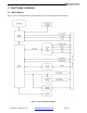
2. FUNCTIONAL OVERVIEW 2.1 Block Diagram Figure 1 shows the ETX-945 COM’s functional blocks, ETX bus, and peripheral interface signals. Figure 1: Functional Block Diagram ETX-945 User Manual 1.00 www.diamondsystems.
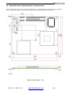
2.2 Board Dimensions, Mounting Holes, and Connectors The two diagrams below show the mechanical dimensions of the ETX-945’s board outline and five mounting holes, as well as the position of all connectors on both the top and bottom sides of the board. Figure 2: Board Layout – Top ETX-945 User Manual 1.00 www.diamondsystems.
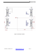
Figure 3: Board Layout – Bottom ETX-945 User Manual 1.00 www.diamondsystems.
2.3 Bus and Interface Connector Summary The ETX-945 has six interface connectors, as listed in the tables below. These connectors are defined in accordance with the ETX 3.0 Computer-on-Module (COM) Specification. Signal functions relating to each of the ETX-945’s interface connectors are discussed in greater detail in Section 4 of this document. 2.4 2.
3. GETTING STARTED This section of the ETX-945 User Manual covers basic hardware setup, power connection, system boot-up, and initial software configuration. First-time ETX-945 users normally receive the product as part of one of Diamond’s Development Kits, which provide everything needed to ensure rapid application development. Important Safe-Handling Information WARNING: ESD-Sensitive Electronic Equipment! Observe ESD-safe handling procedures when working with this product.
3.1 ETX Development Kits To facilitate evaluation and development, the ETX-945 is normally supplied pre-integrated into one of Diamond’s ETX development kits (pictured below). This approach increases project efficiency and reduces risks by providing a known good environment for rapid application development. Diamond’s ETX development kits feature baseboards with I/O connectors for quick and easy access to nearly all system interfaces, a CompactFlash socket, and modular PC/104-Plus expansion.
Using the four long screws provided with the heat-spreader (or heatsink), secure the heat-spreader (or heatsink) to the corresponding standoffs located in the four corners of the top of the ETX-945 module. If the ETX module is to being installed in an enclosure, align the heat-spreader’s (or heatsink’s) corner mounting holes with corresponding hole-pattern on the enclosure before inserting and tightening the four mounting screws.
3.4.3 Advanced Chipset Features From this setup page you can configure the size of the video controller’s on-chip frame buffer, set up the controller’s DVMT (Dynamic Video Memory Technology) mode and memory size, and specify what type of display will be used as the system’s boot-up console output device. DVMT is an advanced video controller function that dynamically allocates system memory to be used as video memory in order to efficiently use of available resources to maximize graphics performance.
3.4.6 PnP/PCI Configuration This section of Setup provides options for configuration of devices connected to the ETX-945’s PCI bus, including the choice between automatic “plug-and-play” (PnP) configuration of IRQ and DMA channel settings. If PnP is disabled, you can specific desired IRQ and DMA channels for PCI devices here. 3.4.7 Other Settings and Utilities A few additional status and control functions are available from Setup’s main menu.
4. INTERFACE CONNECTOR DETAILS This section describes the functions available on all of the ETX-945’s bus and I/O interface connectors. The ETX 3.0 specification, which provides more detail regarding the signals present on the ETX1, ETX2, ETX3, and ETX4 connectors, is available from the ETX Industrial Group’s website (http://www.etx-ig.de/specs/specs.php).
4.1 ETX1 Connector The 100-pin, high-density ETX1 connector implements the board’s PCI bus, USB, and audio signals, as indicated in the table below. Further information regarding each of these signal groups follows the table. (Note: Pins designated “RESERVED” should be left unconnected.
4.1.1 PCI bus signals This set of pins implements the module’s PCI expansion bus. For further information regarding the functions of the PCI bus signals, refer to the PCI Bus Specification, available from the PCI Special Interest Group (http://www.pcisig.com/specifications).
4.1.2 USB signals These pins provide connections to the board’s four USB channels. For further information regarding the functions of the USB signals listed above, refer to the USB 2.0 Specification, available from the USB Implementers Forum (http://www.usb.org). 4.1.
4.1.4 Miscellaneous functions These pins carry power and ground signals and an interrupt request as indicated. Signal Name Signal Function Direction VCC +5V ±5% DC power input In GND Power ground n/a 3V +3.3V ± 5% supply generated on the ETX module, for powering external devices (500mA max. external load) Out RESERVED Do not connect n/a SERIRQ Serial interrupt request In Caution: Do not connect the 3V pins (pins 12 and 16) of EXT1 to an external power source! ETX-945 User Manual 1.
4.2 ETX2 Connector The 100-pin, high-density ETX2 connector implements the board’s ISA bus signals, as indicated in the table below. For further information on the module’s ISA bus signals, refer to the ETX 3.0 Specification.
4.3 ETX3 Connector The 100-pin ETX3 connector implements VGA, LCD (LVDS), TV-video, serial, parallel, floppy, mouse, and keyboard signals. Because pins 51-100 are shared between floppy and parallel port functions, dual signal assignments are indicated in the illustration below. Further information regarding each of these signal groups follows. (Note: Pins designated “RESERVED” should be left unconnected.) .
4.3.1 Analog video output These pins provide video, clock, and sync information for display on analog CRTs, or on LCD flat panels that are compatible with analog CRT timings, as indicated. 4.3.
4.3.3 LCD interface These pins carry data for graphical display on an LCD panel, as indicated. 4.3.
4.3.5 Keyboard, mouse, and infrared transceiver interfaces These pins carry data and clock signals associated with the board’s PS2 keyboard and mouse ports. Additionally, transmit and receive data to/from an IR device, can be routed as indicated. 4.3.6 Signal Name Signal Function Direction KBDAT Data to/from keyboard. In/Out KBCLK Clock signal to keyboard Out MSDAT Data to/from mouse In/Out MSCLK Clock signal to mouse.
4.3.7 Floppy drive interface These pins carry data and control information to/from the board’s floppy drive controller, as indicated.
4.3.8 Miscellaneous functions These pins carry power and ground signals and a GPIO signal, as indicated. Signal Name Signal Function Direction VCC +5V ±5% DC power input In GND Power ground In/Out RESERVED Do not connect n/a LTGIO0 General purpose I/O In/Out ETX-945 User Manual 1.00 www.diamondsystems.
4.4 ETX4 Connector The 100-pin ETX4 connector implements the board’s IDE, Ethernet, and a number of other signals, as indicated in the table below. Further information regarding each of these signal groups follows the table.
4.4.1 IDE interfaces These pins carry data and control information to/from the board’s IDE drive controller, as indicated.
4.4.2 Ethernet port The ETX-945’s 10/100Mbps Ethernet LAN interface signals on connector ETX4 require the use of an external 1:1 transformer. The ETX 3.0 specification provides further details regarding the transformer’s requirements. 4.4.
4.4.4 Miscellaneous signals 2 These pins implement the ETX-945’s I C and SM Bus interfaces, PC-speaker output, and RTC/CMOS backup power input. 4.5 Signal Name Signal Function Direction SPEAKER This logic-level signal can drive a piezoelectric speaker (typically via a transistor) O BATT 2.4V to 3.
5. APPENDIX: SYSTEM RESOURCES REFERENCE 5.1 BIOS Memory Mapping Address Device Description E000:0000h - F000:FFFFh System BIOS Area D000:2000h - D000:FFFFh Free space D000:0000h - D000: FFFh LAN ROM C000:E000h - CF00:FFFFh Free space C000:0000h - C000:DFFFh VGA BIOS A000:0000h - B000:FFFFh VGA RAM 0000:0000h - 9000:FFFFh DOS 640K ETX-945 User Manual 1.00 www.diamondsystems.
5.2 I/O Port Address Map Each peripheral device in the system is assigned a set of I/O port addresses, which also become the identity of the device.
000002E8 - 000002EF Communications Port (COM4) 000002F8 - 000002FF Communications Port (COM2) 00000378 - 0000037F Printer Port (LPT ) 000003B0 - 000003BB Mobile Intel 94 Express Chipset Family 000003C0 - 000003DF Mobile Intel 94 Express Chipset Family 000003E8 - 000003EF Communications Port (COM3) 000003F6 - 000003F6 Primary IDE Channel 000003F8 - 000003FF Communications Port (COM ) 00000400 - 000004BF Motherboard Resource 000004D0 - 000004D1 Motherboard Resource 00000500 - 0000051F Int
5.3 Interrupt Request (IRQ) Lines Peripheral devices use interrupt request lines to notify CPU when services are required. The table below lists the interrupt request channels used by the ETX-945’s onboard devices.
5.4 BIOS POST Codes The POST codes used by the ETX-945’s on-board BIOS appear in the table below.
14h Program chipset default values into chipset. Chipset default values are MODBINable by OEM customers 15h Reserved 16h Initial Early_Init_Onboard_Generator switch 17h Reserved 18h Detect CPU information including brand, SMI type (Cyrix or Intel) and CPU level ( 86 or 686) 191Ah Reserved 1Bh Initial interrupts vector table.
343Bh Reserved 3Ch Test 82 4 3Dh Reserved 3Eh Test 82 9 interrupt mask bits for channel 3Fh Reserved 40h Test 92 9 interrupt mask bits for channel 2 4142h Reserved 43h Test 82 9 functionality 4446h Reserved 47h Initialize EISA slot 48h Reserved 49h Calculate total memory by testing the last double last word of each 64K page; Program writes allocation for AMD K CPU 4A4Dh Reserved 4Eh Program MTRR of M CPU; initialize L2 cache for P6 class CPU and program cacheable range; Initialize
5Dh Initialize Init_Onboard_Super_IO switch; Initialize Init_Onboard_AUDIO switch 5E5Fh Reserved 60h Okay to enter Setup utility 6164h Reserved 65h Initialize PS/2 mouse 66h Reserved 67h Prepare memory size information for function call: INT h ax=E820h 68h Reserved 69h Turn on L2 cache 6Ah Reserved 6Bh Program chipset registers according to items described in Setup and Auto-Configuration table 6Ch Reserved 6Dh Assign resources to all ISA PnP devices; Auto assign ports to onboard COM
82H Call chipset power management hook: Recover the text fond used by EPA logo (not for full screen logo), If password is set, ask for password 83H Save all data in stack back to CMOS 84h Initialize ISA PnP boot devices 85h Final USB initialization; NET PC: Build SYSID structure; Switch screen back to text mode; Set up ACPI table at top of memory; Invoke ISA adapter ROMs; Assign IRQs to PCI devices; Initialize APM; Clear noise of IRQs 8692h Reserved 93h Read HDD boot sector information for Trend